In a modern high-speed design, good component placement can make the difference between whether the design works or fails. The location of a decoupling capacitor, passive component on a differential pair, and even the length of a trace are crucial to design performance. Manually placing components in such a design can be tedious, and while the apps have been developed to assist, such as the PCB Clustering App, significant adjustment is often required. Use AI to quickly place components for PCB layout, optimizing placement and saving time with Allegro X AI, in OrCAD X.
This quick how-to will provide step-by-step instructions on how to use AI to quickly place components for PCB layout with X AI in OrCAD X.
To follow along, download the provided files above the table of contents.
How-To Video
 Open in New Window
Starting X AI
Step 1: Open the provided design in OrCAD X.
Step 2: Select Tools > X AI from the menu to open the X AI panel. This panel can be docked to Presto or undocked and moved anywhere in the canvas.
Step 3: Select Login and enter your Cadence username and password.
Step 4: Select Create New Workspace at the top of the Workspaces panel.
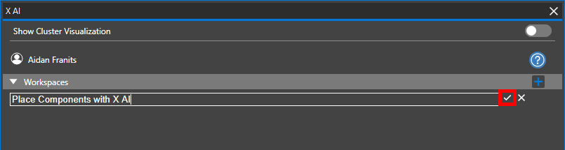
Step 5: Enter a name for the new workspace and click the checkmark button to create it.
Step 6: In the main workspace window, select Upload Board to upload the currently opened board to the X AI server.
Configuring Component Classes
Step 7: Component classes and power/ground layers must be configured properly before components can be placed. Select Setup Component Classes to define unassigned component classes.
Step 8: The Component Classes panel opens with a warning message that reference designators IC.* and X.* are not defined. Add |IC.* to the IC class field.
Note: The | symbol acts as a logical separator and the .* indicates a wildcard.
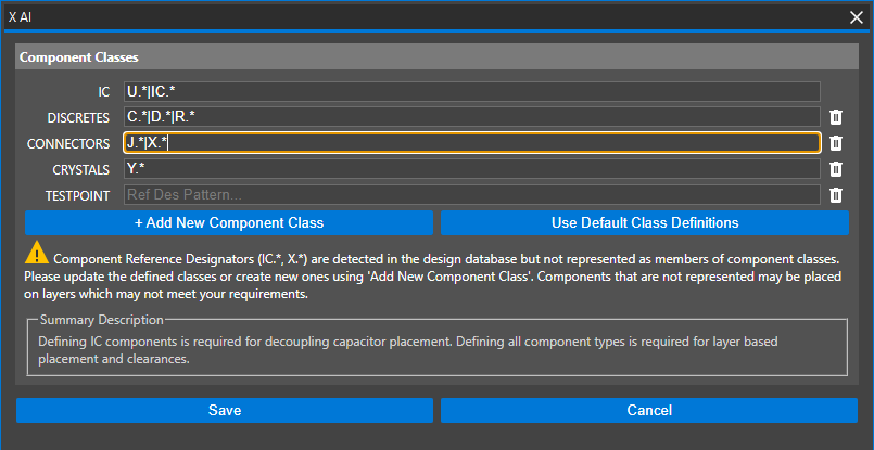
Step 9: Add |X.* to the Connectors field to classify X1 as a connector. Click Save to save the changes and return to the main X AI window.
Configuring Class-Class Spacing
Step 10: Select Class to Class Spacing in the X AI window to configure component spacing settings.
Note: If class-class spacing is not defined, package-to-package collisions may result when components are placed. Learn more about the settings required to get the most out of AI here.
Step 11: In the Class to Class Spacing table, enter 0.254 for the default clearance.
Step 12: Select Autofill Classes. All spacing pairs are listed in the table.
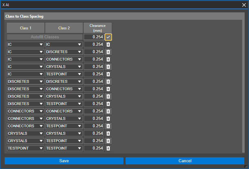
Step 13: Select Apply Default Clearance to apply the defined default clearance to each spacing pair.
Step 14: Click Save to save the settings and return to the main X AI window.
Defining Power and Ground Rules
Step 15: Power and ground placement rules must be defined before components are placed. Select Power and Ground Setup.
Step 16: The Power and Ground Setup table opens. For this design, power and ground net voltages have already been assigned and are listed in the Voltage row.
A prompt is shown, saying that power and ground settings were pre-populated from the design. Click OK to close the prompt.
Step 17: Check the option for POWERPLANE_1 under 3.3V to assign the 3.3V net to the power plane layer.
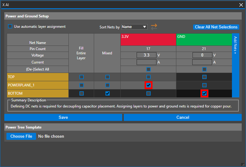
Step 18: Check the option for BOTTOM under GND to assign the ground net to the bottom layer.
Step 19: Click Save to save the settings and return to the main X AI window.
Use AI to Quickly Place Components for PCB Layout
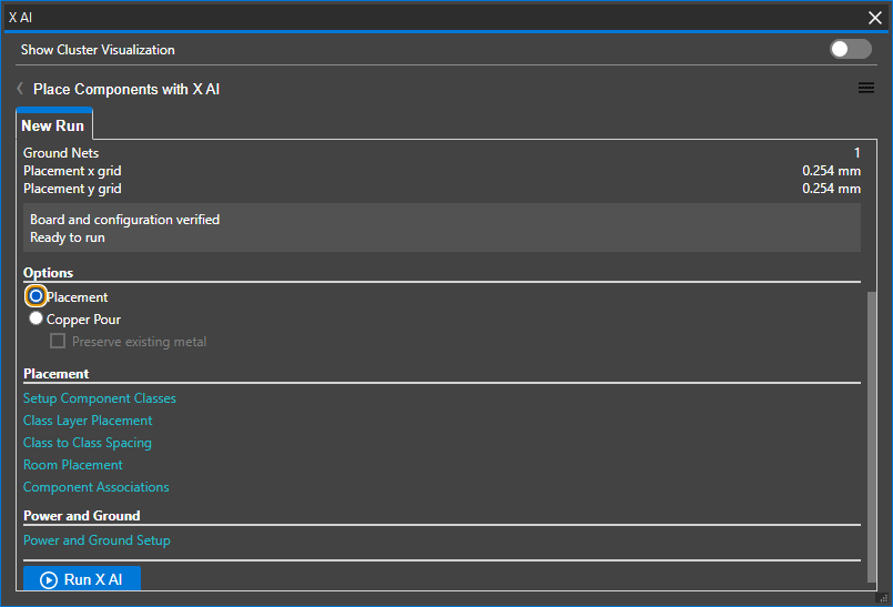
Step 20: With component classes, spacing rules, and power/ground layers defined, components are ready to be placed. Ensure Placement is selected under Options in the X AI panel.
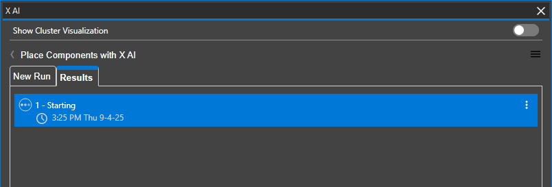
Step 21: Select Run X AI to start placement. The Results tab opens, showing a log of the placement progress.
Step 22: When placement finishes, a green checkmark and a download icon are shown in the run row in the Results table. Click the download icon to download and view the board.
Note: If prompted to save the changes to the existing board, click No.
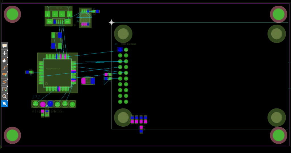
Step 23: View the generated board. The components were placed as shown in the PCB canvas.
Step 24: Review the results and adjust component placement as needed.
Wrap Up & Next Steps
Use AI to quickly place components for PCB layout and accelerate your PCB design process with Cadence X AI in OrCAD X. Learn more about X AI here and get more how-tos for OrCAD X at EMA Academy.

