Accessing a database of accurate, verified symbols and footprints is essential for efficient PCB design; however, model creation and verification for complex components is time-consuming and any errors can have detrimental effects on the functionality of the design. OrCAD Component Information Portal (CIP) directly integrates with Ultra Librarian, allowing users to find and utilize pre-built symbols and footprints for database components.
This quick how-to will provide step-by-step instructions on how to associate and use verified symbols, footprints, and 3D models from Ultra Librarian for new database components in CIP.
How-To Video

Opening CIP
Step 1: In OrCAD Capture CIS, select CIP > Open CIP from the menu.
Step 2: If necessary, log in with your username and password.
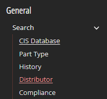
Step 3: Select Search > Distributor from the CIP sidebar menu.
Searching for a New Part
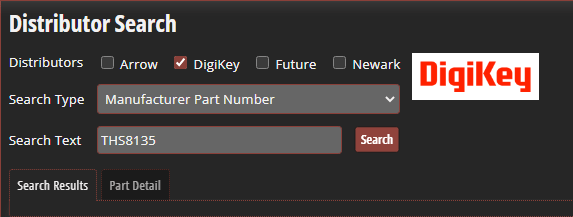
Step 4: Check Digikey as the distributor.
Step 5: From the Search Type drop-down menu, select Manufacturer Part Number.
Step 6: In the Search Text field, type THS8135.
Step 7: Select Search.
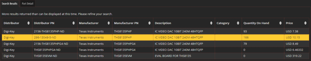
Step 8: From the returned search results, select one of the reported components listed as IC VIDEO DAC.
Accessing Ultra Librarian through CIP
Step 9: Review the component information.
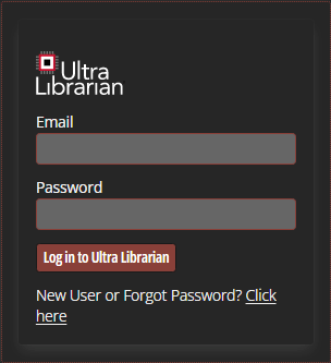
Step 10: In the Ultra Librarian login, enter your username and password and select Log in to Ultra Librarian.
Note: For new Ultra Librarian users, select the Click Here in the Ultra Librarian section to be brought to the registration page.

Step 11: Under the Ultra Librarian integration, select Preview.
Step 12: View the preview of the symbol, footprint, and 3D Model.
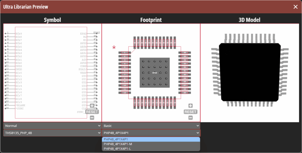
Step 13: For the footprint, select the drop-down menu under Basic to view the additional footprint configurations.
Note: Alternate footprint configurations are available for preview and download for minimum, typical, and maximum pad sizes for footprints according to IPC specifications.
Some components have additional schematic symbols, for example, larger parts with similar-enough sections.
Step 14: For the 3D model, click and drag to rotate the component.
Step 15: Click the X or Close to close the preview.
Adding a Component to the Database
Step 16: Select the Component View drop-down menu and choose ICs.
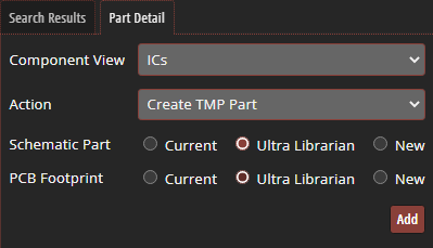
Step 17: Under Action, leave the default Create TMP Part.
Step 18: Under Schematic Part, select the UL radio button.
Step 19: Under PCB Footprint, select the UL radio button.
Step 20: Select Add.
Note: If you receive an error that no library folders are found, Ultra Librarian needs to be configured by an administrator using the following steps:
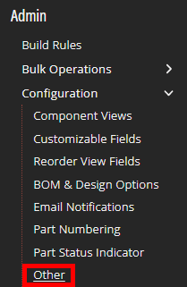
- Select Admin > Configuration > Other from the CIP menu.
- Under Ultra Librarian Configuration Directory, select the pencil to edit.
- Check Enable Common Directory.
- Set the Common Directory paths for Symbols, Footprints, Padstacks, and Step Models.
- Check Save Schematic Symbols to Single OLB.

- Provide a name for the library, such as UL.OLB.
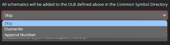
- Under Duplicate Symbol Handling, click the drop-down menu and select the desired action. Admins can choose from:
- Skip to skip the Symbol Generation for duplicate symbols
- Overwrite to overwrite the current symbol with the new symbol
- Append Number to add the duplicate symbol with the addition of a number in the name
- When finished, select the check mark next to Ultra Librarian Common Directory Settings to save the configuration.
Viewing the Component
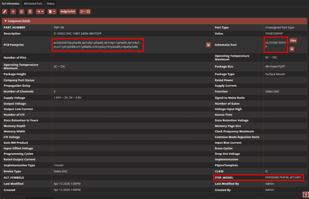
Step 21: View the temporary component. The symbol, footprint, and 3D model have been automatically assigned along with the parametric and distributor information from Digikey.

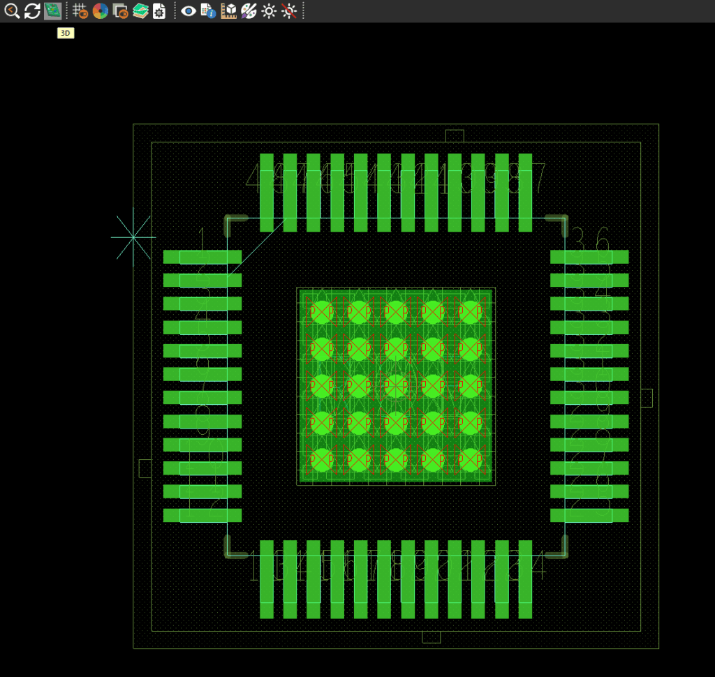
Step 22: Select the PCB Footprint Preview button and click Preview.
Note: If the footprint preview is not configured, select CIP > Settings from the menu. Set the Footprint Viewer Exe to: C:\Cadence\SPB_[version]\tools\bin\allegro_free_viewer_classic.exe.
Step 23: In the PCB canvas, select the 3D icon on the toolbar to view the pre-mapped STEP model.
Step 24: Leave the defaults in the 3D Canvas Filter and click OK.
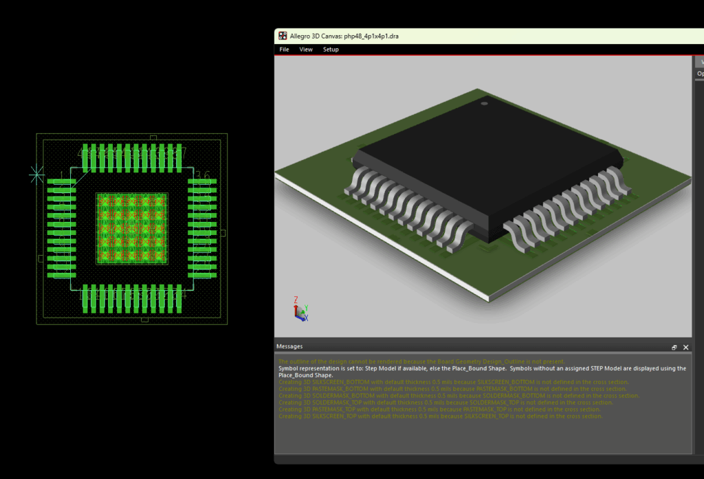
Step 25: View the PCB Footprint and 3D Model.
Step 26: Close the 3D Model and PCB footprint preview.
Step 27: Select the Symbol Preview button.
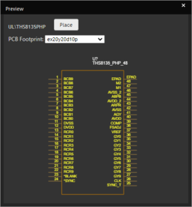
Step 28: View the schematic symbol preview.
Note: If the symbol has multiple sections, select the letters across the top to see each section.
Step 29: Select Place to place the symbol in the schematic canvas.
Step 30: Click to place the schematic symbol in OrCAD Capture CIS. Right-click and select End Mode or ESC on the keyboard when finished.
Note: The temporary part can be utilized in the schematic while the component is reviewed and approved.
Wrap Up & Next Steps
Easily integrate CIP and Ultra Librarian to expedite the PCB design process and ensue accuracy of your database component models. Automatic mapping and download of verified, pre-built symbols, footprints, and 3D models lets you add new components to the database with confidence and quickly continue with the design process.

