Product Description
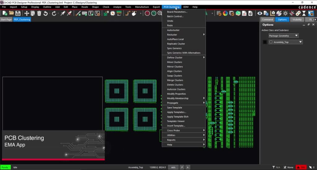
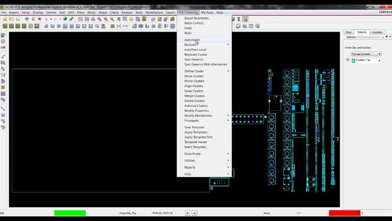
As designs become more complex and project timelines more compressed, it is important to identify opportunities to enhance design processes. PCB Clustering for OrCAD provides AutoClustering technology, intelligent design (IP) reuse, and replication technology that can significantly reduce board placement time. Create functional groups of components based on design information.
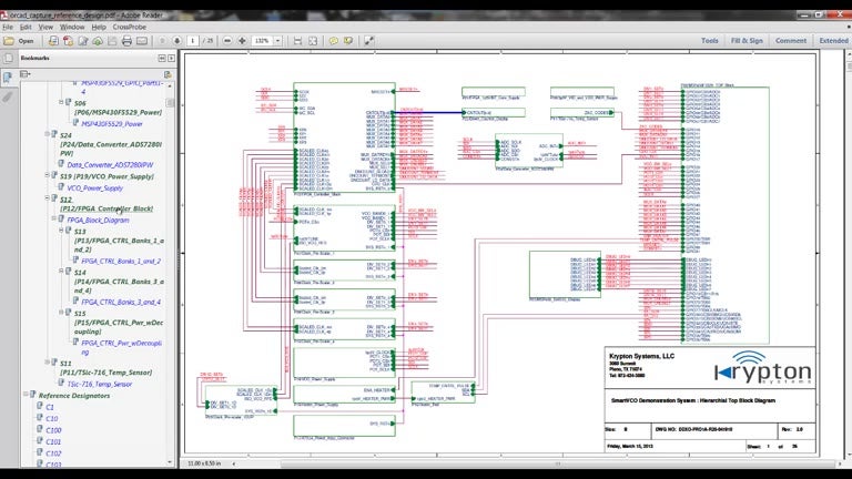
- Cross-Probe between PDF schematic and OrCAD® PCB Editor.
- Create multiple replicas of a source cluster’s net topology.
- Propagate cluster membership, placement, and shape changes to specified clusters.
- Save a design checkpoint at any time and compare it against other checkpoints.
- Create a cluster from a specified group of components.
- Create templates containing a cluster’s membership, net topology, and placement information.
- Propagate cluster reference designator text locations to target clusters.
- Reuse design templates in new or legacy designs.
- Perform early ‘what-if’ spatial analysis using generic circuit templates.