PRODUCT FEATURE

High-Current and High-Power PCB Design

What is High-Current and High-Power PCB Design?

High-current and high-power PCB designs are specialized printed circuit boards engineered to handle large amounts of current, typically used in applications that require the delivery of significant power. These designs are common in power electronics, automotive systems, industrial machinery, and electric vehicles, where components may need to manage currents ranging from several amps to hundreds of amps without overheating, experiencing excessive voltage drop, or compromising performance. High-current PCB designs require specialized techniques to handle significant current loads safely and efficiently. These designs incorporate thicker copper, wider traces, effective thermal management, and strategic layout to maintain functionality under demanding conditions, which is vital for applications in power-intensive industries.

Benefits

  • Compact and Efficient Power Delivery
  • Reduced Power Loss
  • Support for High-Performance Components
  • Enhanced Thermal Management

Try High-Current and High-Power PCB Design with OrCAD X

High-Current and High-Power PCB Design in OrCAD X

High-Current PCB designs require additional considerations to ensure safety and reliability. OrCAD X includes the functionality required to design and analyze your high-current and high-power PCB designs with:
  • Efficient Copper Layers and Plane Definition
  • Constraints definition for high-current traces and vias
  • Thermal Reliefs
  • Customizable Stackup Materials
  • Trace Shielding
  • Rules for Component and Trace Spacing

Key Features of High-Current and High-Power PCB Design in OrCAD X

OrCAD X and Allegro X contain the functionality you need to accurately and efficiently complete your high-current and high-power PCB designs.
Thermal Relief Definition and Management
Easily define thermal reliefs in the design by configuring the type, minimum and maximum values, and width as user defined or based upon constraint values. The visual graphic provides context as to which type of thermal relief you are configuring to guarantee it is the correct selection for your design.
Copper Pours and Planes
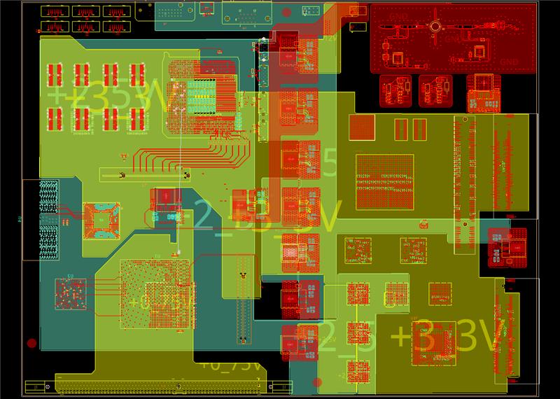
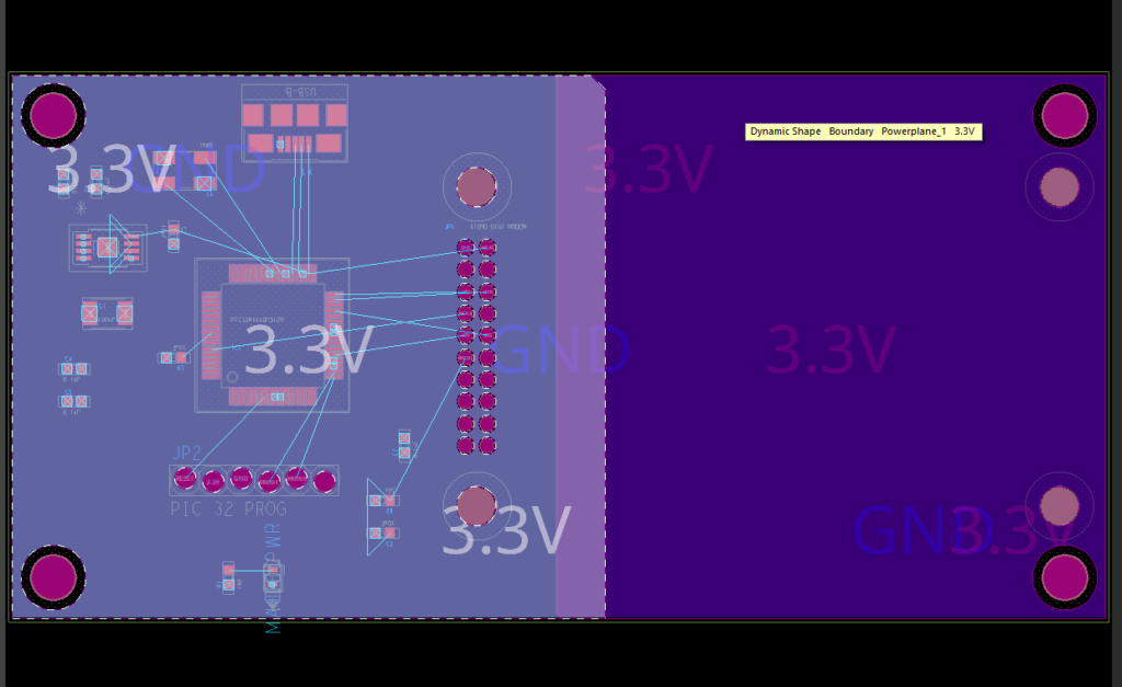
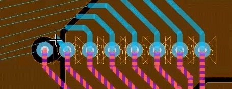
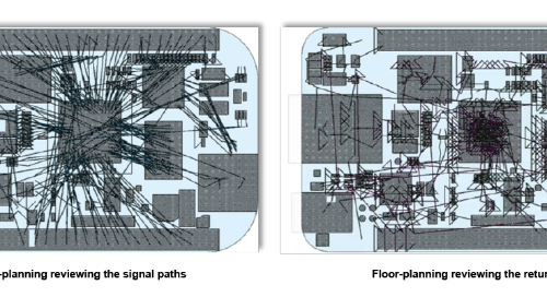
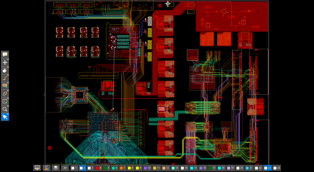
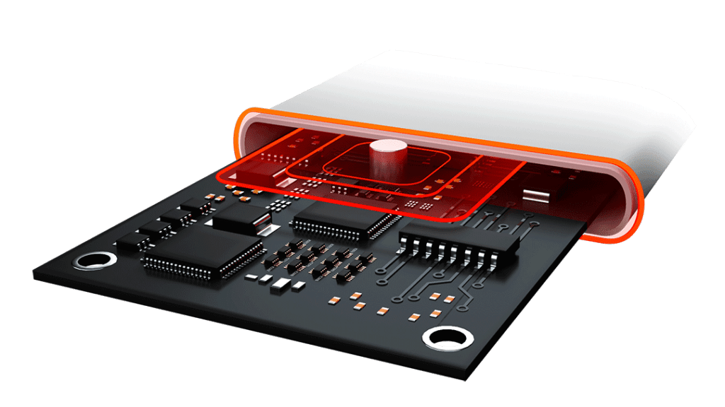
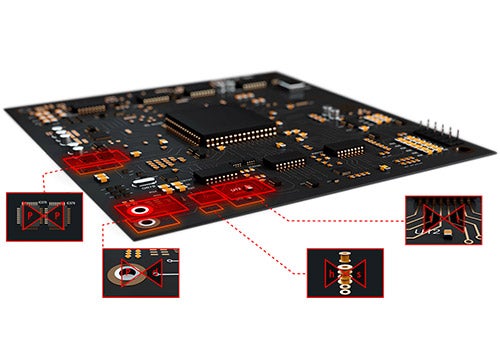
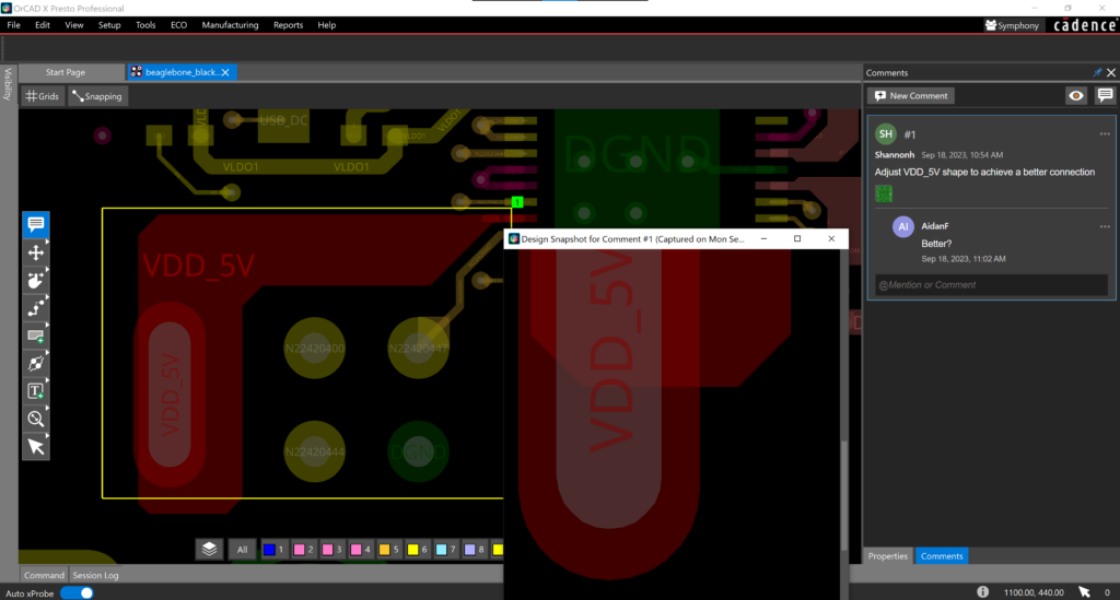
For high-current, high-power PCB designs a robust and continuous power delivery network is essential. OrCAD X provides efficient methods to create copper pours and planes including shape creation (rectangular, polygon, and circle), copy and paste methods, void creation, and more.
Customizable Materials
It is important to define the exact materials used in the PCB stackup to ensure proper fabrication and even more so if simulations are being performed to verify PCB functionality. OrCAD X includes a vast list of materials to select from to define the layers in the PCB and enables the definition of custom materials and properties to accurately detail the required stackup.
Constraint Definition and Management
The comprehensive constraint manager in OrCAD X enables designers to configure rules for trace width, neck width, spacing, and vias to accommodate the current carrying capacity requirements for high-current and high-power nets. Physical and spacing requirements are automatically applied to nets when routing and any errors are flagged in real-time to ensure safety requirements are met efficiently.
Class to Class Spacing Rules
Ensure high-current features have adequate spacing and remain separated throughout the PCB layout with class to class spacing rules. Easily define the UL or VDE spacing requirements and OrCAD X will automatically check the spacing between nets and identify any violations.

Get the PCB Design Capabilities You Need Today and Tomorrow

Let our team help you craft the perfect PCB design solution for your requirements. Contact us for more information.

Additional Resources for High-Current and High-Power PCB Design

Leverage the Advanced Capabilities of OrCAD X

Learn more about the advanced features and capabilities of OrCAD X that will help you design your PCBs quickly and accurately.

Related Features

EMA Design Automation