PRODUCT FEATURE

RF PCB Design

What is RF PCB Design?

RF (Radio Frequency) PCB design focuses on creating circuit boards for applications operating at high frequencies, typically above 100 MHz and into the GHz range. These boards are crucial in telecommunications, radar systems, satellite communications, WiFi, Bluetooth, cellular technology, and other wireless communications applications. Due to the high frequencies involved, RF PCB design demands precise handling of signal integrity, impedance control, and electromagnetic interference (EMI) to maintain signal quality and minimize losses.

Benefits

  • Enhanced Connectivity for Modern Applications
  • Integration of High-Frequency Components
  • Minimal Signal Loss
  • High-Performance Designs

Try RF PCB Design with OrCAD X

RF PCB Design in OrCAD X

OrCAD X and Allegro X enable you to incorporate RF aspects into your designs to ensure a robust, high-performing PCB. OrCAD X and Allegro X provide efficient integration of high-frequency components such as filters, antennas, and amplifiers along with functionality critical to RF PCB design creation including:
  • Impedance constraints and impedance matching
  • Customizable RF stackup material
  • Integration to RF simulation tools
  • Trace Shielding
  • Design Rule Definition with Real-Time Feedback
  • Thermal Management Support
  • Via Shielding
  • Signal Integrity Analysis
  • Trace Antenna and Spiral Inductor Design

Key Features of RF PCB Design in OrCAD X

OrCAD X and Allegro X contain the functionality you need to accurately and efficiently complete your RF PCB designs.
Pro
Via Shielding
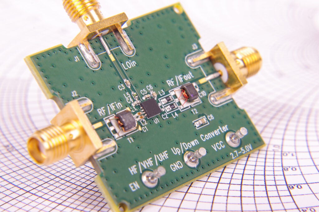
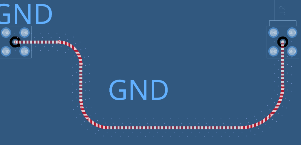
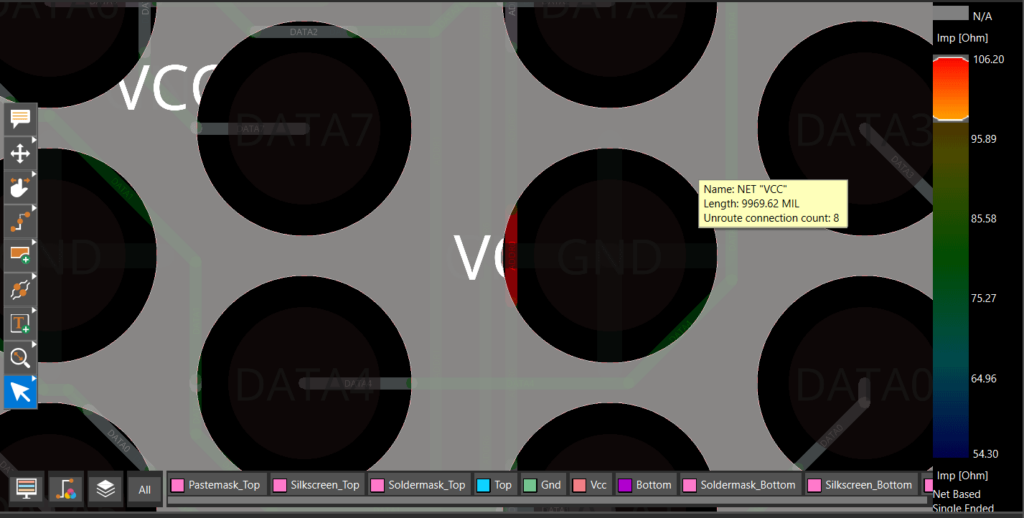
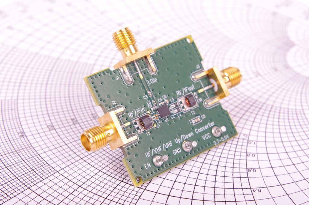
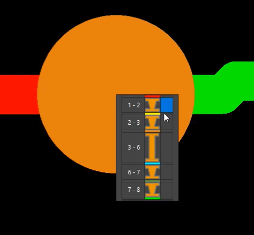
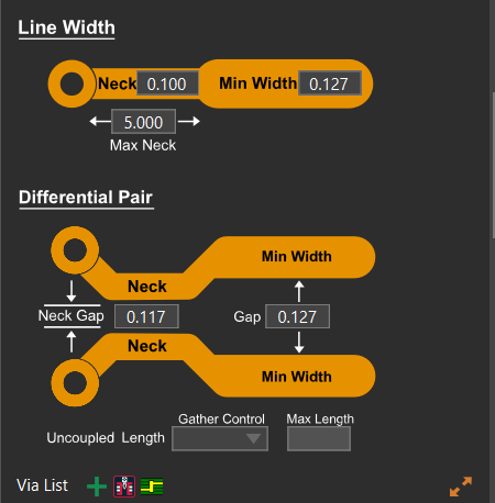
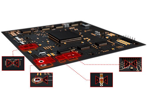
Quickly create via arrays around traces, shapes, and sensitive areas of the PCB with an easy-to-use widget. Graphics provide a visual aid to understand the parameter definition of your via shielding and allow you to easily define gaps, offsets, row counts, nets, vias, and more to accurately create the via shielding required for your sensitive RF signals.
Pro
Signal Integrity Analysis
Perform signal integrity analysis to evaluate signal coupling and impedance discontinuities directly in the PCB canvas. OrCAD X provides integrated coupling and impedance analysis with tabular results and color-coded overlays- helping you identify common SI issues throughout the PCB layout.
Impedance Control
Easily define rules for impedance requirements in your RF designs to ensure the source and load impedance match in your RF systems. OrCAD X allows you to define and assign impedance constraints to nets in the design and provides real-time feedback when routing the PCB to ensure impedance requirements are met throughout the layout process.
DXF Import
Quickly import your RF structures with DXF import in OrCAD X. Easily define the DXF file, units, and map layers between the DXF file and PCB design to quickly and accurately import your RF structures.
Create Shapes From Lines
Compose shapes from lines and arcs to build the complex shapes required for your RF PCB designs. OrCAD X allows you to convert lines, which can be imported from a DXF file, then define the class, subclass, and net to create unique shapes on the PCB.
Constraint Management
Easily define and manage the complex rules required for your RF designs with the extensive constraint manager in OrCAD X. OrCAD X contains comprehensive rules for spacing, traces, vias, impedance, tolerances, and more. Design rule checks are performed in real-time throughout the PCB layout, allowing you to identify and correct any issues as you design when change is easiest.

Get the PCB Design Capabilities You Need Today and Tomorrow

Let our team help you craft the perfect PCB design solution for your requirements. Contact us for more information.

Additional Resources for RF PCB Design

Leverage the Advanced Capabilities of OrCAD X

Learn more about the advanced features and capabilities of OrCAD X that will help you design your PCBs quickly and accurately.

Related Features

EMA Design Automation