As data rates continue to increase and signal margins become increasingly constrained, understanding the electrical behavior of high-speed interconnects has become essential to successful PCB design. While schematics define connectivity, they do not capture the physical characteristics of the routed PCB that ultimately determine signal performance. Trace geometry, via transitions, return paths, termination components, and routing topology can all significantly influence signal integrity.
Topology extraction bridges the gap between physical layout and electrical analysis by converting the actual PCB interconnect structure into an accurate electrical model. By extracting the real signal path directly from the layout database, engineers can perform detailed signal integrity analysis using the true physical implementation rather than an idealized representation. This enables earlier identification of potential issues, more accurate simulations, and greater confidence that high-speed interfaces will perform as intended.
What is Topology Extraction?
Topology extraction is the process of automatically identifying and converting the physical interconnects in a PCB layout into an electrical model that can be used for signal integrity, power integrity, and timing simulations.
Topology extraction generates an S-Parameter model that can be used for additional time-domain simulation and analysis. It extracts the actual signal path from the PCB database and creates a representation of the network topology for analysis. A topology extraction process typically identifies:
- Driver and receiver devices
- PCB traces and their lengths
- Trace widths and layer assignments
- Via locations and transitions
- Branches and stubs
- Connectors and cables
- Package models
- Termination components
- Reference planes and return paths
- Net topology, including point-to-point, daisy-chain, fly-by, or star configurations
Common Uses of Topology Extraction

Topology extraction can be used to identify potential signal integrity issues on the extracted topology of a signal net. Once a topology is extracted, transient simulation can be performed, and results can be analyzed, including:
- Time-domain waveforms
- Eye diagrams
- Signal quality parameters
Why Should You Perform Topology Extraction?
Topology extraction should be performed when a layout-based extraction for the topology is required in your PCB designs, for example if analysis is needed for high-speed signals. Using an S-parameter model from a topology extraction has several benefits including:
- Increased Accuracy:
Quickly create realistic, highly accurate, power-aware S-Parameter models for system-level simulation. Greater customization allows you to incorporate decoupling capacitors and termination resistance into models.
- Pre-Layout and Post-Layout Analysis:
Extracted topologies can be used to perform general purpose pre-layout and post-layout exploration of signals and custom system-level topologies.
- Channel Simulation and Verification:
High-speed serial and parallel interfaces must perform channel simulation and verification to ensure design intent. Extracting topologies will enable you to incorporate accurate models into the channel simulation for a realistic analysis.
How to Extract Board Topologies
The following method can be employed to extract topologies:
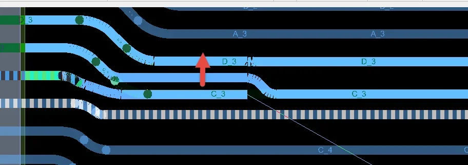
Step 1: Select and review the desired nets
After routing is completed, select the net or Xnet that requires additional analysis. Obtain and review a 3d view of the net topology including the position on the PCB, layer, via transition, and trace parameters such as the width.
Step 2: Extract the Topology
Once the desired nets have been selected and reviewed, extract the topology from the PCB layout database to generate an electrical representation of the signal path.
Step 3: Modify the Topology
Ensure nodes are connected, terminate unconnected pins, and map external models to increase accuracy such as IBIS-AMI models.
Step 4: Perform SI and Additional Analysis
Define the transient simulation parameters such as step size, time, data rate, number of bits, stimulus pattern and more. Perform the required additional analysis and analyze the waveform results.
Step 5: Design Modifications
Adjust the PCB layout as required to improve signal quality of high-speed nets based on the SI analysis, such as modifying routing or termination strategies.
Following this process allows engineers to create accurate electrical models of their high-speed nets and validate signal behavior before fabrication. However, manually preparing topologies, assigning models, configuring simulations, and interpreting results can be time-consuming, particularly for complex designs with numerous critical nets. As signal speeds increase and design schedules become more compressed, reducing the effort required to perform topology extraction and signal integrity analysis becomes increasingly important, this is where Sigrity Aurora can help.
Topology Extraction with Sigrity

Sigrity Aurora automatically extracts topology directly from the PCB layout database, allowing engineers to investigate signal behavior using the actual physical design rather than an idealized representation. Performing topology extraction in Sigrity Aurora:
- Eliminates manual creation of simulation models
- Reduces setup time for SI analysis
- Prevents modeling errors
- Captures actual PCB routing effects
- Allows rapid investigation of design changes
- Enables early detection of signal integrity issues
- Provides a uniform, cohesive environment for PCB layout, topology extraction, and SI analysis
By automating topology extraction directly from the PCB layout database and providing guided workflows for simulation and analysis, Sigrity Aurora enables designers to quickly investigate signal behavior, identify potential issues, and implement design improvements earlier in the layout process.
Learn more about topology extraction using Sigrity Aurora with our free course: Introduction to In-Design SI/PI analysis with Sigrity Aurora.