PCB design reuse is the practice of capturing validated circuit blocks, layout modules, and schematic templates as managed assets and reusing them in new designs. Done correctly, it cuts weeks off a schedule and prevents repeated work on common circuits. However, doing it haphazardly or incorrectly creates version control issues that compound over time. In this article, we will look at the following:
- Why PCB design reuse reduces schedule risk: How capturing validated circuit blocks in a managed library eliminates repeated work and preserves engineering IP across projects.
- Best practices for a structured reuse strategy: The shift from informal copy-paste habits to a governed data ecosystem, including how to standardize component libraries and maintain compliant hierarchical blocks.
- Executing reuse with OrCAD X: How OrCAD Reuse Modules and OrCAD Template Management translate methodology into a repeatable workflow, from schematic capture through component placement.
| PCB Design Reuse Comparison: Informal vs. Managed | ||
| Factor | Informal Copy-Paste | Managed Reuse (OrCAD) |
| Version control | None, file-based | Centralized, revision-tracked |
| Preserved layout intent | No | Yes, via Reuse Modules |
| Constraint transfer | Manual re-entry | Automatic with the module |
| Team scalability | Single engineer | Enterprise-wide |
| Onboarding speed | Slow | Fast, documented assets |
Understanding the Value of PCB Design Reuse
Copying circuit blocks from old schematics is common but can be tricky. Notably, that approach breaks when components go obsolete, source files change, or the original designer is unavailable. A more reliable method is to implement PCB design reuse through a version-controlled library of validated blocks, where each entry retains its routing constraints, layout intent, and verification history.
The core benefits fall into three areas:
- Cycle time reduction: A validated power block that takes days to design and simulate can be reused in minutes. Across multiple projects, this time adds up quickly.
- Risk reduction: A block that has passed EMC and thermal validation retains that data. The risk shifts to new circuitry rather than to repeated sections.
- IP preservation: When proven designs are stored in a managed library, they remain accessible regardless of team changes.
Common Reuse Challenges
The main problems are version control, setup, and adoption. Shared folders without access control or change history push engineers back to old files. Initial setup is also a barrier: defining block boundaries, documenting validation status, and migrating existing circuitry into a managed library takes upfront effort that teams often deprioritize under schedule pressure. Once that foundation is in place, experienced designers will not change habits unless the new flow saves real time. A structured system solves both by making the managed path easier than copy-paste.
Best Practices for Implementing a PCB Design Reuse Strategy
Successful implementation requires moving away from informal habits and toward a formal data ecosystem. Focus on these three core areas to build a reliable library that engineers will actually use.
Shift from Copy-Paste to Managed Data
Start by identifying circuit blocks used in more than two designs, such as power rails, oscillator networks, CAN interfaces, and USB-C front ends. These are the first candidates for reuse modules.
Notably, each block should include validation status, target PCB stackup, layout constraints, and component versions. Without this data, reuse introduces risk instead of reducing it.
Standardize Component Libraries and Hierarchical Blocks
Reuse breaks when the same component appears as different symbols across multiple libraries. A unified component library with a single symbol, a single footprint, and verified parameters is required for reliable reuse.
Hierarchical schematic blocks should follow a naming convention that reflects their function and revision. A block named “PWR_3V3_LDO_v2” communicates more than “power_block_final.” The naming convention enforces discipline without requiring constant oversight.
Govern the Data Across the Enterprise
For reuse to scale beyond a single team, the library needs:
- a defined owner
- a change review process
- a mechanism for pushing updates to dependent designs
Without governance, the library drifts: some teams use v1 of a block, others use v3, and no one knows which is current. The data management layer is what converts a local practice into an enterprise capability.
Executing PCB Design Reuse with OrCAD Template Management
Setting up and transitioning to a formal strategy requires the right toolset to bridge the gap between design theory and physical reality. OrCAD X provides this through two mechanisms: Reuse Modules, which capture and transfer both schematic and layout data as a single linked asset, and templates, which standardize board-level settings like stackups, design rules, and constraint sets across new projects.
For example, a power management block saved as a reuse module carries its placement, routing, and constraints directly into the new PCB editor session. At the same time, a product-family template ensures that the new board starts with the correct layer count and impedance rules already in place. Together, these workflows eliminate the manual reconstruction that is both slow and error-prone in informal reuse.
OrCAD Reuse Modules in Practice
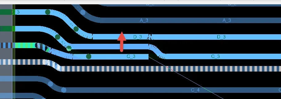
OrCAD X addresses PCB design reuse directly through Reuse Modules, which allow engineers to capture schematic blocks and their associated layout as linked, reusable assets. When a reuse module is instantiated in a new design, it carries the original placement, routing, and constraints.
The workflow is simple. Save a validated block as a reuse module in OrCAD X and store it in a central database. When needed, place it from the library into the schematic, and the layout appears in the PCB editor with placement intact. This also extends to similar circuitry, since OrCAD X can map differing components between the module and the target circuit. In effect, that means a validated block does not need to be an exact match to be useful.
OrCAD Template Management for Consistency
OrCAD X handles the design-level layer of reuse through templates and technical files. Board templates carry predefined stackups, design rules, constraint sets, and layer configurations. A new PCB project that starts from a validated template inherits all of those settings immediately, eliminating a category of setup errors that typically surface late in the design cycle.
For organizations running multiple product lines with different stackup requirements, maintaining a template per product family keeps these configurations controlled and auditable.
Templates can also be created and applied to manufacturing documentation in LiveDoc, accelerating the documentation creation process.
Setting Up a Unified Design Database in OrCAD
Storing reuse modules and templates in a centralized OrCAD database gives every engineer on the team access to the same validated assets in real time. When a block is updated, the change is immediately visible across the organization, without manually redistributing files or notifying individual designers.
This setup also enforces IP sharing by design: instead of knowledge sitting in a single engineer’s project folder, it lives in a governed repository that the whole team can draw from. For multi-site teams, this means a hardware engineer in one office can instantiate and trust the same power rail block that a colleague qualified in another location.
Implementing PCB Design Reuse with OrCAD X
PCB design reuse at the methodology level produces measurable gains in schedule, quality, and intellectual property (IP) retention. Unified libraries, governed data, and managed hierarchical blocks form the foundation.
Template management functionality and reuse modules provide a direct way to implement these practices in OrCAD X. They enable teams to store validated designs, control revisions, and reuse schematic and layout data without rework.
If your team is still using shared folders and project copies, move to a managed system. EMA Design Automation provides OrCAD X tools, integration support, and training for teams implementing PCB Design Reuse. Contact EMA to review your current workflow and identify gaps in your PCB Design Reuse process.
EMA Design Automation is a leading provider of the resources that engineers rely on to accelerate innovation. We provide solutions that include PCB design and analysis packages, custom integration software, engineering expertise, and a comprehensive academy of learning and training materials, which enable you to create more efficiently.
For more information on PCB Design Reuse and how we can help you or your team innovate faster, contact us.