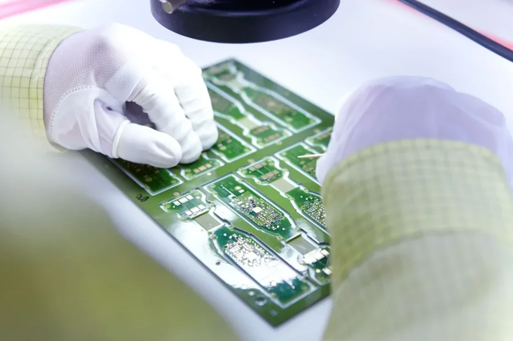
For Engineering Managers and VPs, the hardware development cycle is a constant battle between schedule, budget, and quality. In this equation, the “re-spin”, a physical iteration of the printed circuit board required to fix errors, is often treated as an inevitable cost of doing business.
However, modern data suggests that the acceptance of multiple re-spins is a legacy mindset that drains profitability. With the complexity of modern high-speed designs (DDR5, PCIe Gen5, 112G), the cost of PCB design spins has ballooned. It is no longer just a few hundred dollars for a new bare board; it is tens of thousands of dollars in lost time, materials, and market opportunity. This article quantifies the Return on Investment (ROI) of shifting from a “build-test-fix” methodology to a simulation-driven “correct-by-construction” workflow using advanced EDA tools.
The Anatomy of a Re-spin Cost
When estimating the cost of PCB design spins, many teams make the mistake of counting only the “hard costs,” the invoice from the fabrication house and the assembly provider. This is only the tip of the iceberg. According to industry estimates, the average cost of a re-spin for a moderately complex, high-speed board ranges from $10,000 to $50,000 per iteration. Here is the breakdown of that figure:
- Hard Costs (20%): Fabrication (NRE, expediting fees), Components (wastage, rush shipping), and Assembly labor.
- Engineering Labor (30%): The “burn rate.” If three senior engineers (EE, Layout, SI) spend two weeks debugging, root-causing, and redesigning, that is tens of thousands in salary overhead diverted from the next revenue-generating project.
- Lab & Testing Overhead (10%): Utilization of thermal chambers, EMC compliance testing facilities, and specialized measurement equipment.
- Opportunity Cost (40%): The most damaging factor. If a product launch is delayed by a month due to a spin, you lose a month of peak sales volume that can never be recovered.
Traditional vs. Advanced EDA Workflows Comparison
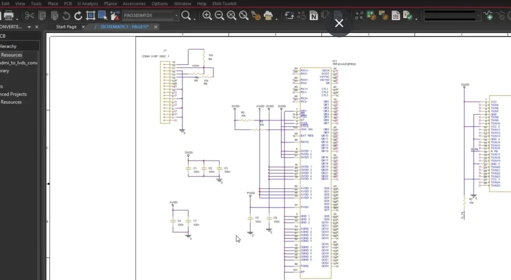
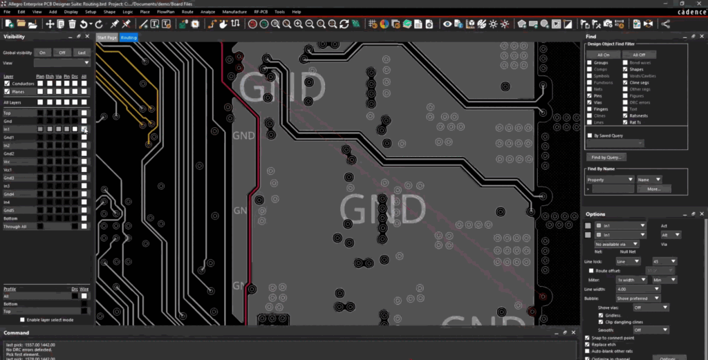
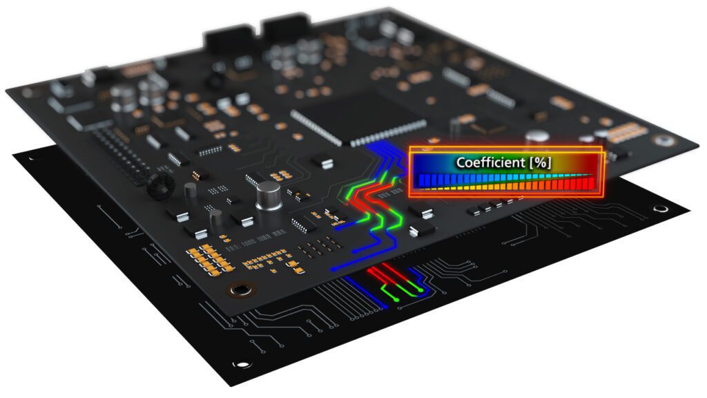
The primary driver of excessive spins is the workflow itself. The traditional workflow relies on physical prototyping to find errors. The advanced EDA workflow uses integrated analysis (SI/PI/Thermal) to virtually detect errors.
Impact of Workflow on Design Iterations
| Metric | Traditional Workflow (Build-Test-Fix) | Advanced Workflow (Simulation-Driven) |
| Verification Method | Physical Lab Testing / Oscilloscopes; Prototyping | Virtual Simulation with Integrated Signal Integrity, Power Integrity, and Thermal Analysis |
| Avg. Spins to Production | 4.6 | 3.0 |
| Error Discovery | Post-Fab (High Cost) | Pre-Fab (Low Cost) |
| Design Cycle Impact | High unpredictability | Predictable closure |
The Time-to-Market (TTM) Multiplier
The true cost of a silicon re-spin is not just in the fabrication, but also the lost time. A single complex re-spin typically consumes ~4 weeks, including root-cause analysis, redesign, fabrication, assembly, and validation. By eliminating two re-spins, an advanced workflow recovers 8 weeks of development time.
- For Engineering Managers: 8 weeks of schedule and engineering budget preserved.
- For VPs and Executives: A product launch two months earlier.
In consumer electronics and fast-moving IoT markets, a two-month Time-to-Market advantage can be the difference between market leadership and irrelevance.
Calculating the Cost of PCB Design Spins
The true cost of PCB design spins is the sum of hard expenses, engineering burn rate, and the often-overlooked opportunity cost. You can estimate the liability of your current workflow using the following formula:
Where:
- Hard Costs (Direct Expenses): Fabrication NRE, board spin materials, assembly costs, expedited shipping fees, and scrapped components.
- Engineering Labor: The number of engineering hours spent debugging, root-causing, re-layouting, and re-verifying, multiplied by the hourly burden rate of the team.
- Opportunity Costs (Lost Revenue): The potential revenue or market share lost for every week the product launch is delayed.
A Real-World Scenario
Let’s apply this formula to a typical high-speed, moderate-volume project to visualize the impact.
Scenario: A PCIe Gen5 Interface Card
- Hard Costs: $12,000 (Expedited fab/assembly for 10 prototypes).
- Soft Costs: 3 Engineers (Hardware, Layout, SI) x 80 hours each x $100/hr = $24,000.
- Opportunity Cost: The product is projected to generate $50,000 in monthly margin. A single spin delays launch by 4 weeks (1 month) = $50,000.
Total Cost for ONE Re-Spin:
By adopting advanced analysis tools that enable first-pass success (1 spin), you can effectively save $172,000 per project directly to the bottom line. These savings far exceed the cost of the software license required to achieve that result.
Reducing the cost of PCB design spins is not just an engineering objective; it is a business imperative. The data clearly shows that “saving money” by skipping simulation software is a false economy. The cost of a single avoided spin often exceeds the cost of the software required to prevent it.
EMA Design Automation is a leading provider of the resources that engineers rely on to accelerate innovation. We provide solutions that include PCB design and analysis packages, custom integration software, engineering expertise, and a comprehensive academy of learning and training materials, which enable you to create more efficiently. For more information on the cost of PCB design spins and how we can help you or your team innovate faster, contact us.