The Internet of Things (IoT) is a buzz word hard to avoid in today’s technical society. Known as the biggest thing since the .com boom, IoT increases connect-ability between the physical and digital worlds. IoT has often been referred to as the “infrastructure of the information society” and has led to intelligent connected platforms for innovative devices such as wearables, home automation, and medical monitoring products. Connected devices can be sensed and controlled remotely, improving efficiency, accuracy, and economic gain. As a result, new approaches to PCB design have emerged as well.
How does IoT drive new PCB approaches?
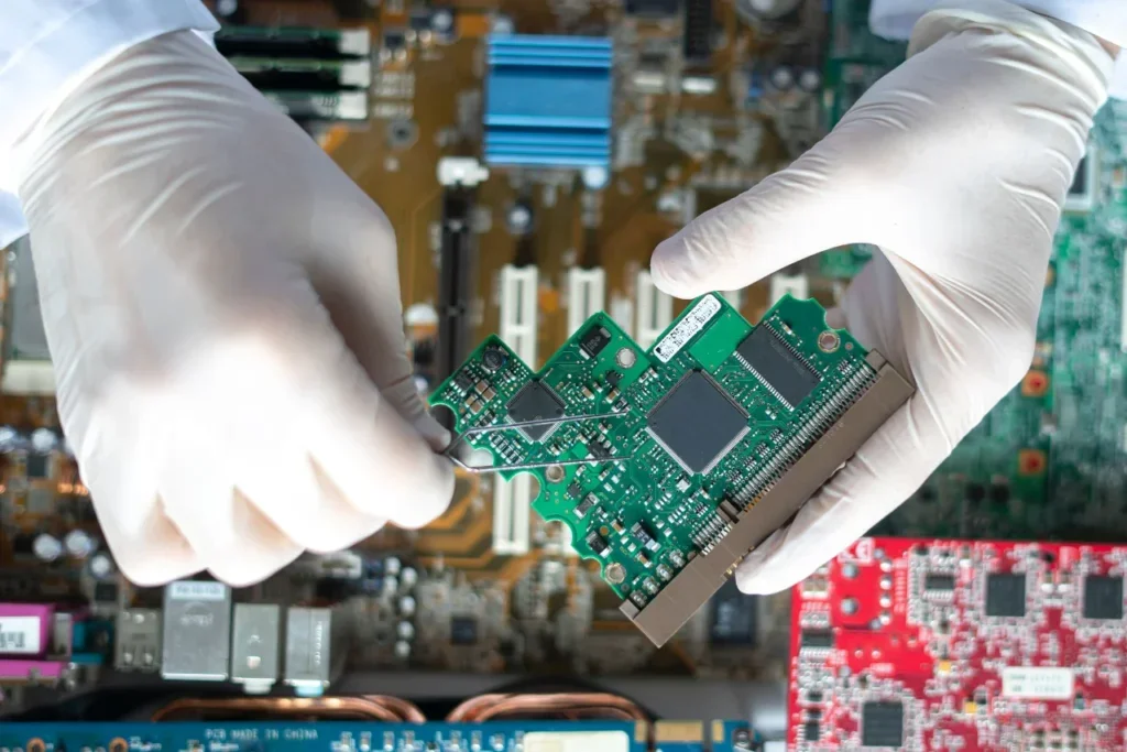
The PCB world is rapidly innovating to keep up with consumer demands. People are increasingly interested in devices that are smaller yet process information at a faster rate driving new approaches to PCB design. In order for devices to be both smaller and connect to the IoT, flex and high density interconnect (HDI) PCBs have increased in demand.
Flex PCBs are ideal for fitness trackers and other small devices as more components can be added to a smaller space. The use of flex PCBs simplifies complicated wiring and provides extra resistance when exposed to harsh conditions. As board real estate decreases and routing density goes up, HDI techniques such as blind and buried vias are used to achieve routing closure. HDI design approaches have also lead to lower power consumption and higher performance, making them ideal for IoT devices.
By combining flex and HDI approaches to PCB designs, companies now have the ability to create smaller devices without compromising performance. This combination leads to improved reliability of PCBs through the reduction of issues such as thermal stress and improved signal quality. IoT devices now have the ability to be smaller, lighter and faster, however designers must still be aware of certain design requirements.
Design Requirements for IoT Applications
- Extended Battery Life: IoT devices are always on and constantly communicating with the network. Working to extend battery life through product design is an important factor to consider. As a result analyzing power integrity and optimizing power consumption during the design phase has become a common requirement.
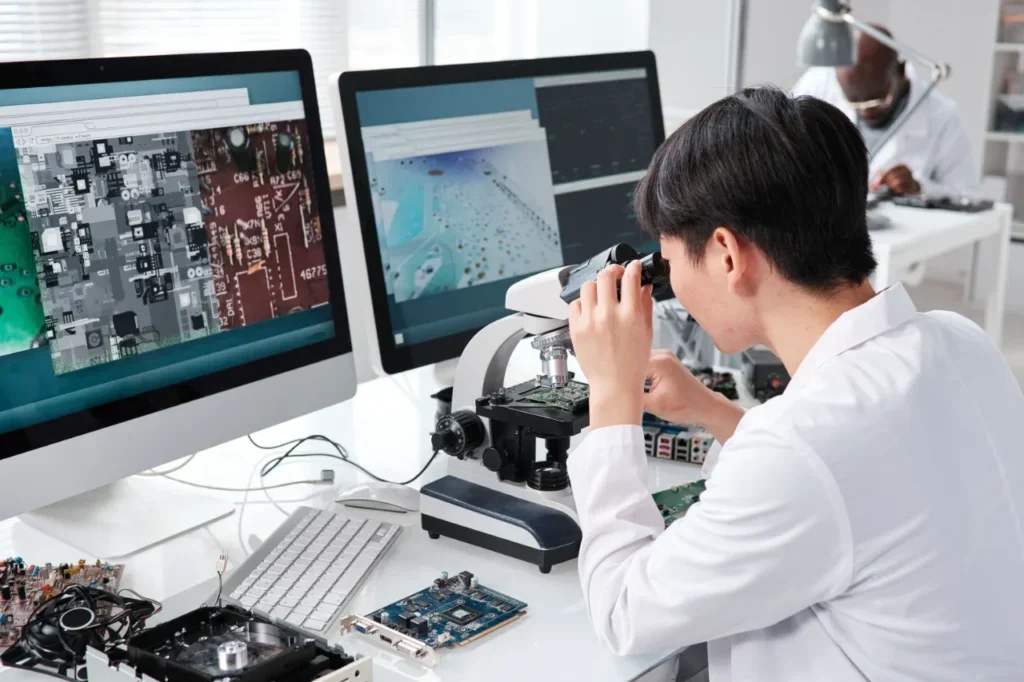
- High Standards: As consumers become dependent on their IoT devices, the industry standards of reliability are expanding. Users want to be able to trust that their device remains operational and accurate as the IoTs rapidly changes over time. As a result PCB designers will rely more on simulation programs such as PSpice to virtually prototype their design in software across a wide variety of potential conditions to increase reliability and help to optimize their designs.
- Security: As millions of devices are connected to the IoT, developers believe that updating security through software will not be enough and suggest implementing hardware based security mechanisms to offer added protection of information.
- Size & Flexibility: Most IoT applications are small by necessity. Physical limitations such as size and flexibility, are increasingly important aspects to keep in mind while designing for IoT. Approaches such as rigid-flex and HDI help designers meet the functionality requirements of these connected devices while conforming to smaller form factor devices
Meeting the IoT Challenge
As the IoT continues to evolve, PCB designers have a responsibility to stay current on trends in order to understand its impact on PCB design. By being aware of certain restrictions and requirements necessary to build connected IoT devices, designers will have a better sense of how to design the most effect PCBs on the market.