As electronics continue to shrink, engineers face growing challenges in routing increasingly dense components. Standard plated-through-holes cannot always accommodate modern fine-pitch layouts, making it practical to learn how to design high-density interconnect (HDI) PCBs to maximize routing density. Because HDI uses laser-drilled microvias, very thin dielectrics, and tight trace widths to pack more functionality into a smaller footprint, the move to HDI requires careful layout planning, smart material choices, and strict design rules.
How to Design High-Density Interconnect (HDI) PCBs: Stackups and IPC-2226
Stackups dictate the physical base of your board. The IPC-2226 standard sorts HDI stackups into several types. Designers commonly use the i+N+i naming setup. Here, the letter “i” stands for the number of buildup layers on each side, while the letter “N” stands for the central core. That means for a basic 1+N+1 setup, you have one layer of microvias where the vias connect the outer layers to the first inner layer.
When breaking out heavy ball grid arrays (BGAs), you often need a 2+N+2 stackup, which requires two pressing cycles. You drill the core, press the first buildup layer, drill again, and repeat. Each pressing cycle adds manufacturing complexity and cost, so build expenses climb quickly as additional lamination steps are introduced.
IPC-2226 HDI Stackup Types and Typical Applications
| IPC-2226 Type | Common Notation | Via Structures | Typical Application |
|---|---|---|---|
| Type I | 1+N+1 | Microvias (blind) + PTH | Simple boards, single-layer breakouts |
| Type II | 1+N+1 | Microvias, blind, buried + PTH | Moderate density, limited surface area |
| Type III | 2+N+2 | Microvias (multiple layers), blind, buried | Fine-pitch BGAs (0.4mm to 0.5mm) |
IPC-2226 defines six HDI types in total. Types IV through VI apply to coreless and passive-substrate constructions used in advanced semiconductor packaging rather than standard PCB design and are outside the scope of this guide.
Microvias and Thermal Physics
Microvias are the main feature of HDI design. Standard drills typically go down to around 0.34 mm. By contrast, HDI relies on lasers to burn away dielectric material, forming holes of 0.10 mm or smaller. Even so, the aspect ratio remains a major factor for good yields. For reliable plating, keep the microvia depth-to-diameter ratio below 0.75:1 to ensure copper plating within the hole.
When managing multiple HDI layers, you face a choice. You can use stacked or staggered microvias:
- Staggered vias offset each microvia connection to different layers. The connections look like a staircase.
- Stacked vias sit right on top of each other.
Consider thermal physics for a moment. Stacked vias save space on the board. However, the structure concentrates mechanical stress. During wave soldering or reflow, the board gets hot. This causes the copper and the resin to expand at different rates.
As a result, stacked microvias can literally tear apart under such thermal stress. Notably, the IPC issued a formal warning about hidden defects in stacked microvias. Staggering the microvias takes up slightly more room, but it significantly improves reliability testing results.
Blind and Buried Vias
HDI designs also use blind and buried vias alongside microvias. Blind vias connect an outer layer to one or more inner layers without passing through the entire board. Buried vias connect only internal layers and remain completely enclosed within the PCB. Designers use these structures to free routing channels while avoiding the space consumed by full through-holes.
Fine-Pitch Routing and Signal Integrity
High-density routing focuses strictly on managing physical space and maintaining signal integrity.
When dealing with 0.4 mm pitch BGAs, standard fanouts fail mechanically. Instead, you must use via-in-pad technology, which places the microvia directly inside the component landing pad. The fabricator then plates the hole shut, then sands the surface completely flat, freeing up massive routing paths on the inner layers and allowing the decoupling capacitors to sit directly under the processor.
From an electrical standpoint, HDI provides several electrical advantages for high-speed designs:
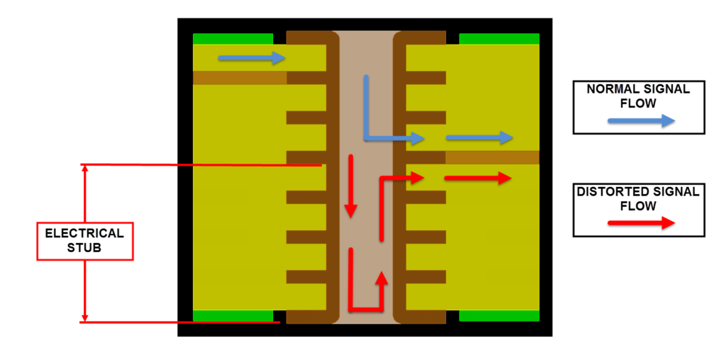
- Elimination of Via Stubs: Standard through-holes leave via stubs behind. A via stub acts like a tiny antenna. The metal stub reflects high-frequency signals, causing noise and severe signal loss. Microvias remove the physical stubs entirely.
- Reduced Parasitics: The very short electrical path of a microvia significantly reduces unwanted parasitic capacitance and internal inductance.
- Tighter Impedance Control: Managing line impedance becomes much easier. The physical distance to the reference plane drops to just 2 or 3 mils.
- Lower PDN Impedance: Thin dielectric layers inherently drop the power distribution network (PDN) impedance. Lower PDN impedance results in cleaner power delivery across the board.
Material Selection
Selecting the right core and prepreg heavily influences your final factory yields. Traditional FR4 woven glass often struggles under direct laser drilling. Further, the thick glass bundles physically deflect the laser beam. Deflection leaves uneven, jagged hole walls. Consequently, designers specify dielectrics formulated precisely for high-density architectures.
When planning the stackup, engineers target specific material properties:
- Laser-Drillable Prepregs and RCC: Resin Coated Copper (RCC) and spread-glass prepregs offer a highly uniform medium. The consistent resin allows the laser to burn clean, predictable holes.
- High-Tg Limits: High glass transition temperature (Tg) resins are fundamentally required. The fabricated board must withstand multiple intense lamination-pressing cycles without peeling or delaminating.
- Halogen-Free Compounds: Electronic designers frequently mandate halogen-free laminates, which meet strict environmental regulations and limit toxic outgassing during thermal breakdown.
- ABF (Ajinomoto Build-Up Film): For leading-edge HDI in consumer electronics and advanced packaging, Ajinomoto Build-up Film (ABF) offers superior laser drillability and finer line/space capability compared to RCC, and is now the dominant buildup material at advanced process nodes.
Cost Tradeoffs vs. Density Benefits
Every layer added to an HDI board increases build costs. Laser drilling time, extra pressing cycles, and special materials inflate the final price. However, the density benefits often justify the expense.
A standard 12-layer through-hole board can often be reduced to an 8-layer HDI board.
Dropping four physical layers reduces the overall board thickness and weight, benefiting aerospace, medical, and mobile products.
Understanding how to design high-density interconnect (HDI) PCBs means knowing when to absorb build costs for system-level gains. For example, a smaller board footprint lets engineers fit more boards on a single factory panel. More boards per panel drive down the per-unit cost. The initial sticker shock of HDI fades when you factor in the system savings.
Real-World Examples
HDI delivers the greatest value when routing density, electrical performance, or board size limits make conventional multilayer PCBs impractical. We see their impact in applications such as:
- Consumer electronics: Smartphones, tablets, and wearables use HDI with fine-pitch BGAs and via-in-pad technology to maximize routing density while minimizing board size.
- High-reliability systems: Aerospace, medical, networking, and automotive electronics use HDI to improve signal integrity, reduce weight, and package complex circuitry into compact designs.
Design for Manufacturability (DFM)
Design for Manufacturability (DFM) and Design for Testability (DFT) practices keep production efficient. In HDI design, you spend more on advanced board builds, yet you save money on the overall system cost. Working closely with your board maker early in the layout phase prevents nasty surprises. Always establish clear design rules before placing the first component.
Fabrication houses require specific clearances to ensure high yields. Consider the following parameters when setting DFM limits:
- Trace Width and Spacing: HDI allows lines as small as 2 mils. Ensure the factory can etch such fine features without bridging.
- Annular Ring Limits: Microvias need a sufficient capture pad. IPC standards generally require a minimum annular ring of 1 mil after plating.
- Solder Mask Expansion: Tight component spacing leaves very little room for solder mask webs. Specify exact tolerances to prevent solder bridging.
- Drill to Copper Clearances: Keep internal copper layers far enough away from laser-drilled holes to avoid plating shorts
Common HDI Design Pitfalls
Poor HDI design decisions can reduce fabrication yields, increase costs, and create long-term reliability issues. Common pitfalls include:
- Exceeding fabrication capabilities: Specifying trace widths, spacing, or microvia dimensions beyond the manufacturer’s process limits.
- Overusing stacked microvias: Excessive stacking increases mechanical stress and the risk of interconnect failure during thermal cycling.
- Choosing unsuitable materials: Standard laminates may not support reliable laser drilling or repeated lamination cycles.
- Ignoring signal return paths: Poor reference plane continuity degrades signal integrity and increases EMI.
- Delaying DFM and DFT reviews: Waiting until the layout is complete often leads to costly redesigns and manufacturing delays.
Design for Testability (DFT) Constraints
Testing an HDI board presents unique physical hurdles. For example, bed-of-nails testers cannot easily hit fine-pitch pads. DFT requires planning for test points on the outer layers wherever possible.
As a result, boundary scan testing via JTAG is highly recommended for dense BGAs, which verifies the internal connections of integrated circuits. The scan works without requiring physical test probes on every single net.
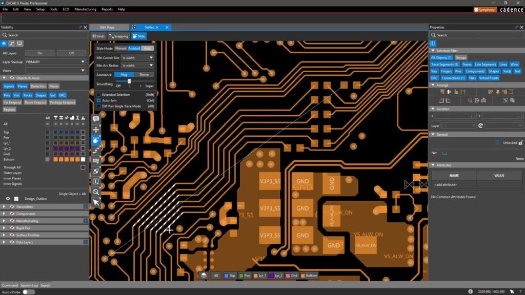
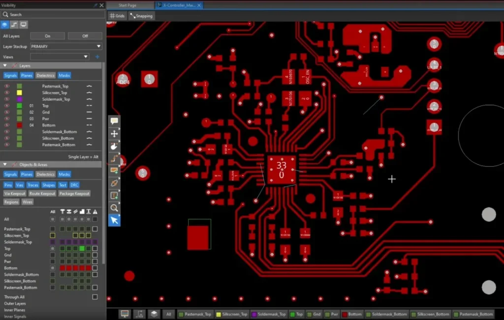
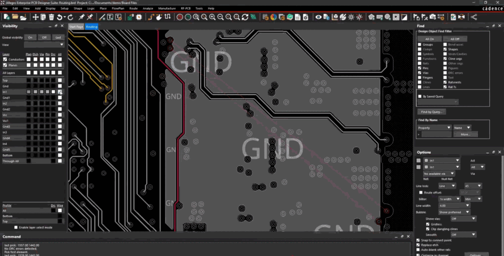
Modern toolchains are absolutely necessary for high-speed layout. Software suites like Cadence OrCAD X handle complex rule management. Setting up trace spacing and clearance rules correctly keeps the design within factory limits. Rules-driven layout software prevents costly board respins.
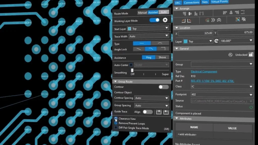
Features like dynamic copper pouring and automatic via staggering speed up the routing phase. Engineering teams rely on advanced EDA tools to verify electrical performance and simulate thermal stress. Using real-time 3D clearance checking ensures dense component placement avoids physical crashes on the factory floor.
Beyond electrical testing, HDI designs undergo reliability validation to confirm long-term interconnect performance. Common methods include thermal cycling, X-ray inspection of hidden interconnects, cross-section analysis of plated microvias, and interconnect stress testing (IST) to verify via integrity under repeated thermal loading.
Practical HDI PCB Workflow
To review, designing an HDI PCB follows a structured process that balances electrical performance, manufacturability, and production cost. The following workflow helps engineers reduce layout iterations while improving fabrication yields and long-term reliability:
- Plan the stackup: Define the layer count, dielectric materials, controlled impedance targets, and microvia structure with your fabricator.
- Place critical components: Position fine-pitch BGAs, memory devices, and high-speed interfaces before routing begins.
- Complete escape routing: Use microvias, blind vias, buried vias, or via-in-pad where appropriate to fan out dense packages efficiently.
- Route critical signals and power: Maintain impedance targets, minimize discontinuities, and optimize the power distribution network.
- Verify the design: Perform signal integrity, power integrity, thermal, and design rule checks before releasing the layout.
- Review DFM and DFT requirements: Confirm the design meets fabrication capabilities and includes adequate test access before manufacturing.
Learning how to design high-density interconnect (HDI) PCBs requires precision, proven methods, and the right engineering software. EMA Design Automation provides industry-leading EDA tools, training, and engineering services to help you conquer complex layouts. Equip your team with the technical skills needed to bring advanced electronic products to market faster. Visit EMA Design Automation today to explore software solutions tailored for your next HDI project.
EMA Design Automation is a leading provider of the resources that engineers rely on to accelerate innovation. We provide solutions that include PCB design and analysis packages, custom integration software, engineering expertise, and a comprehensive academy of learning and training materials, which enable you to create more efficiently. For more information on how to design high-density interconnect (HDI) PCBs and how we can help you or your team innovate faster, contact us.