PCB Design
How to Define Differential Pairs in the Schematic
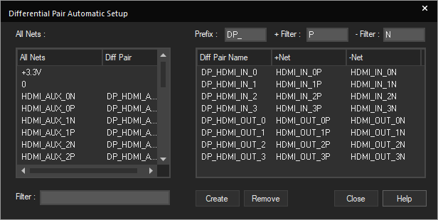
Learn how to define and configure differential pairs during the schematic both manually and automatically in OrCAD Capture.
Learn how to define and configure differential pairs during the schematic both manually and automatically in OrCAD Capture.
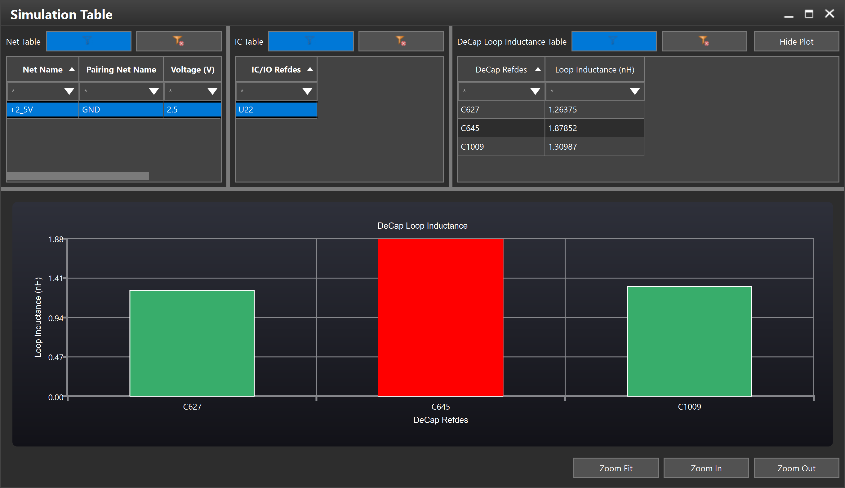
Learn how to analyze loop inductance and improve decoupling capacitor performance using the power inductance workflow in Sigrity Aurora.
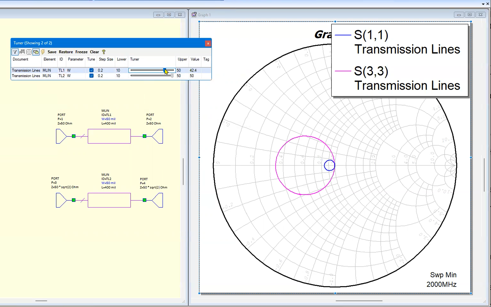
Learn how to design transmission lines & match impedance values to meet Wilkinson Power Divider requirements with AWR RF Design & Simulation.
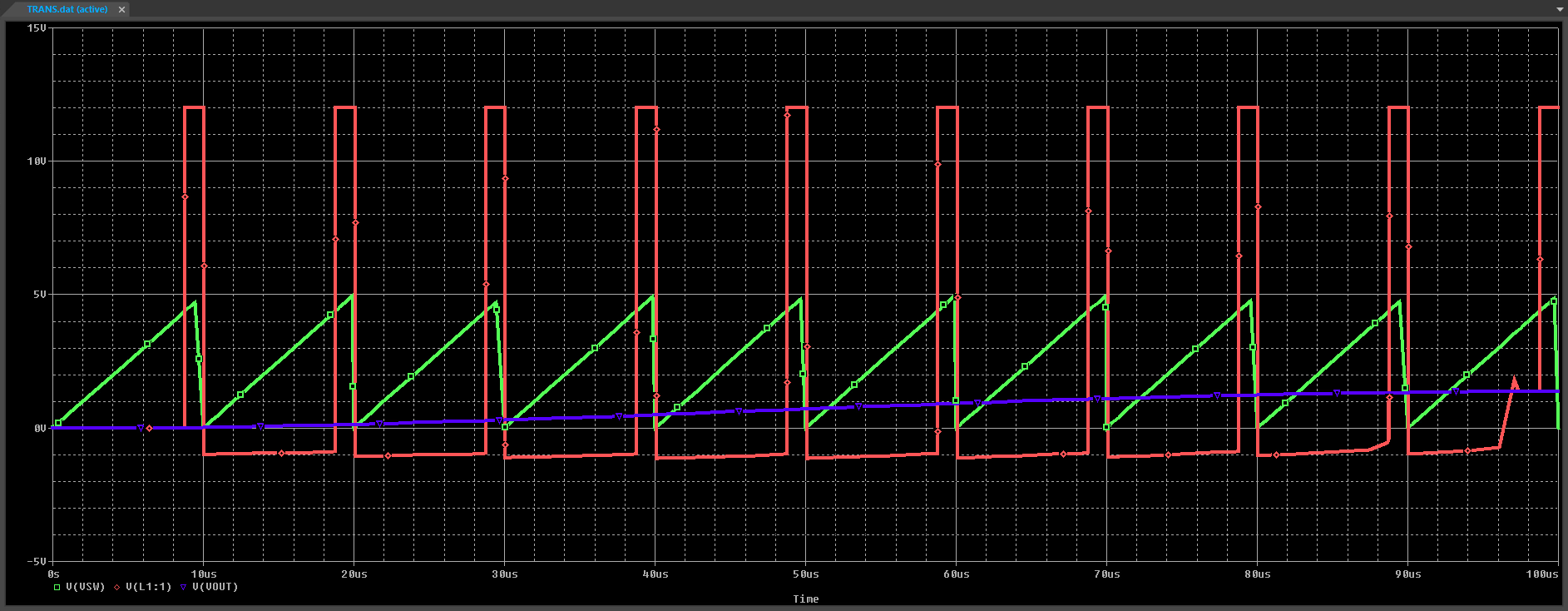
This step-by-step guide will teach you how to create a switch SPICE model for realistic circuit simulation and analysis.
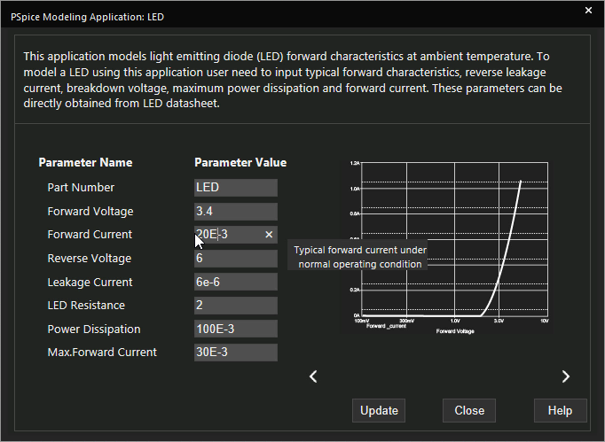
This step-by-step guide will teach you how to create an LED SPICE Model for realistic circuit simulation and analysis.
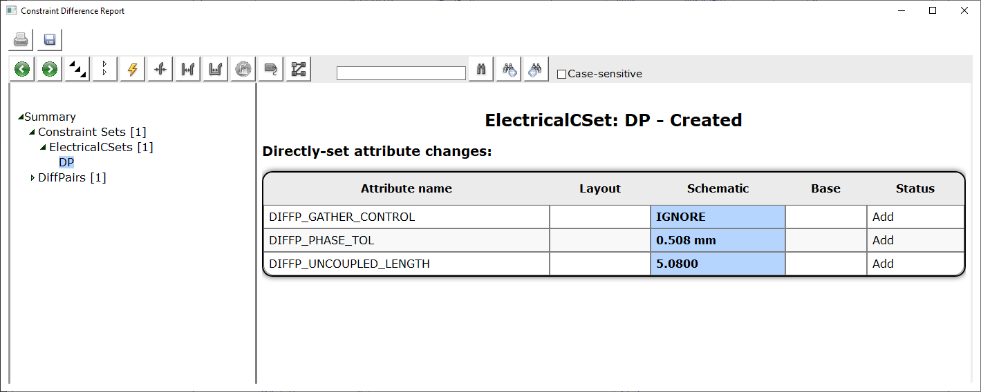
Learn how to synchronize constraints between OrCAD PCB Editor and OrCAD Capture to accurately communicate design intent.
This step-by-step guide will teach you how to create a Pulse source SPICE Model for use in circuit simulation.
This step-by-step guide will teach you how to create a Piecewise linear (PWL) SPICE model for use in PSpice.
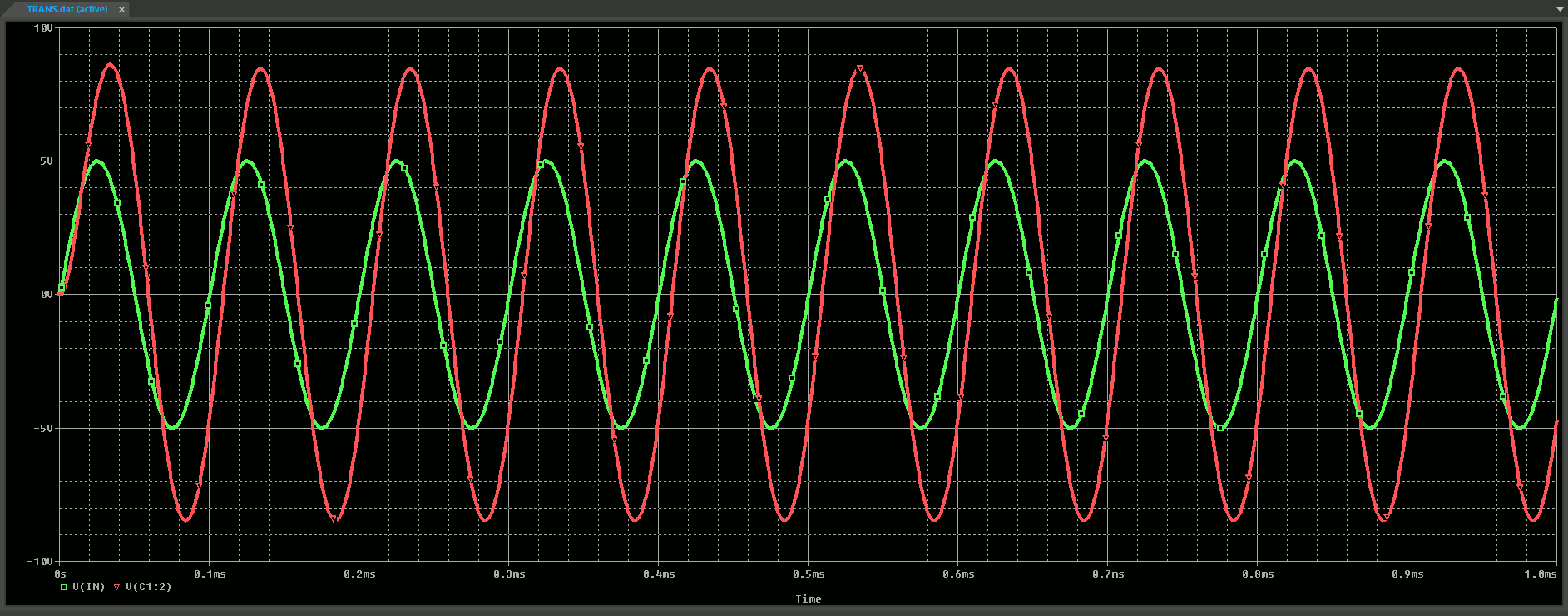
This how-to will provide step-by-step instructions on how to create a Sine Source SPICE Model to simulate and analyze circuit behavior.
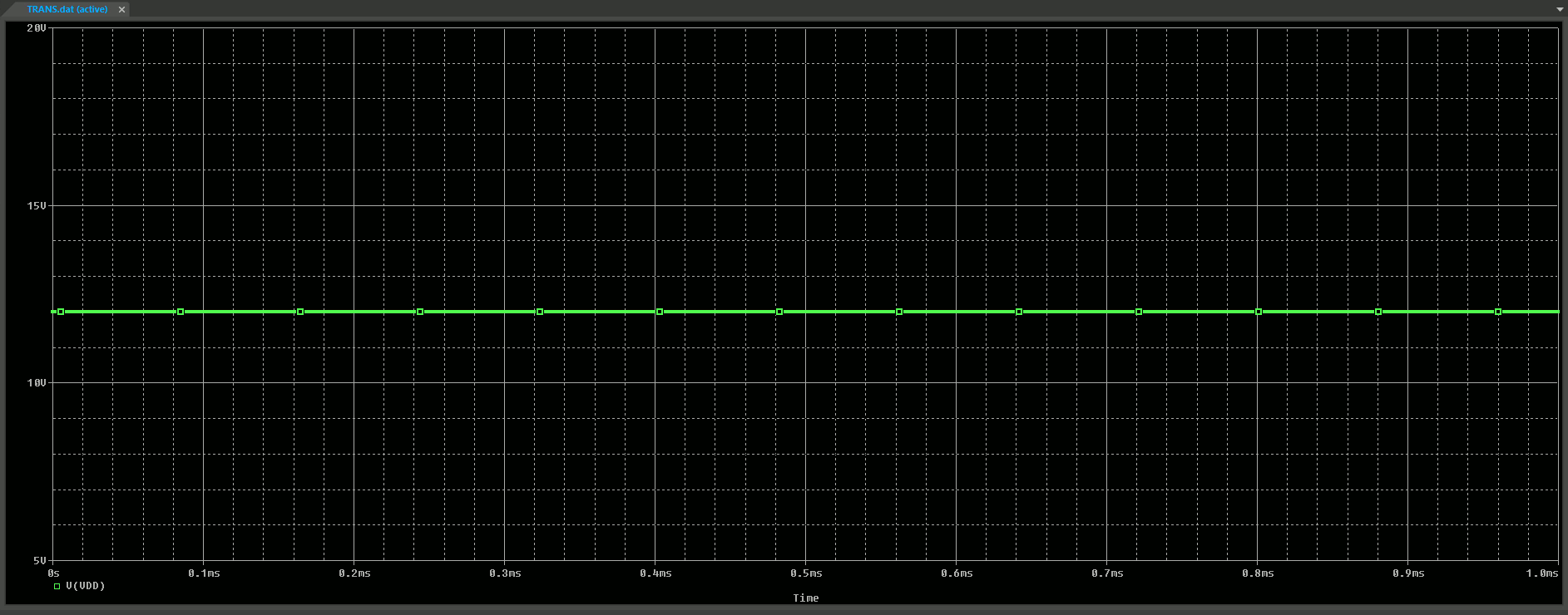
This how-to will provide step by step instructions on how to create a DC Source SPICE Model to simulate and analyze circuit behavior.