
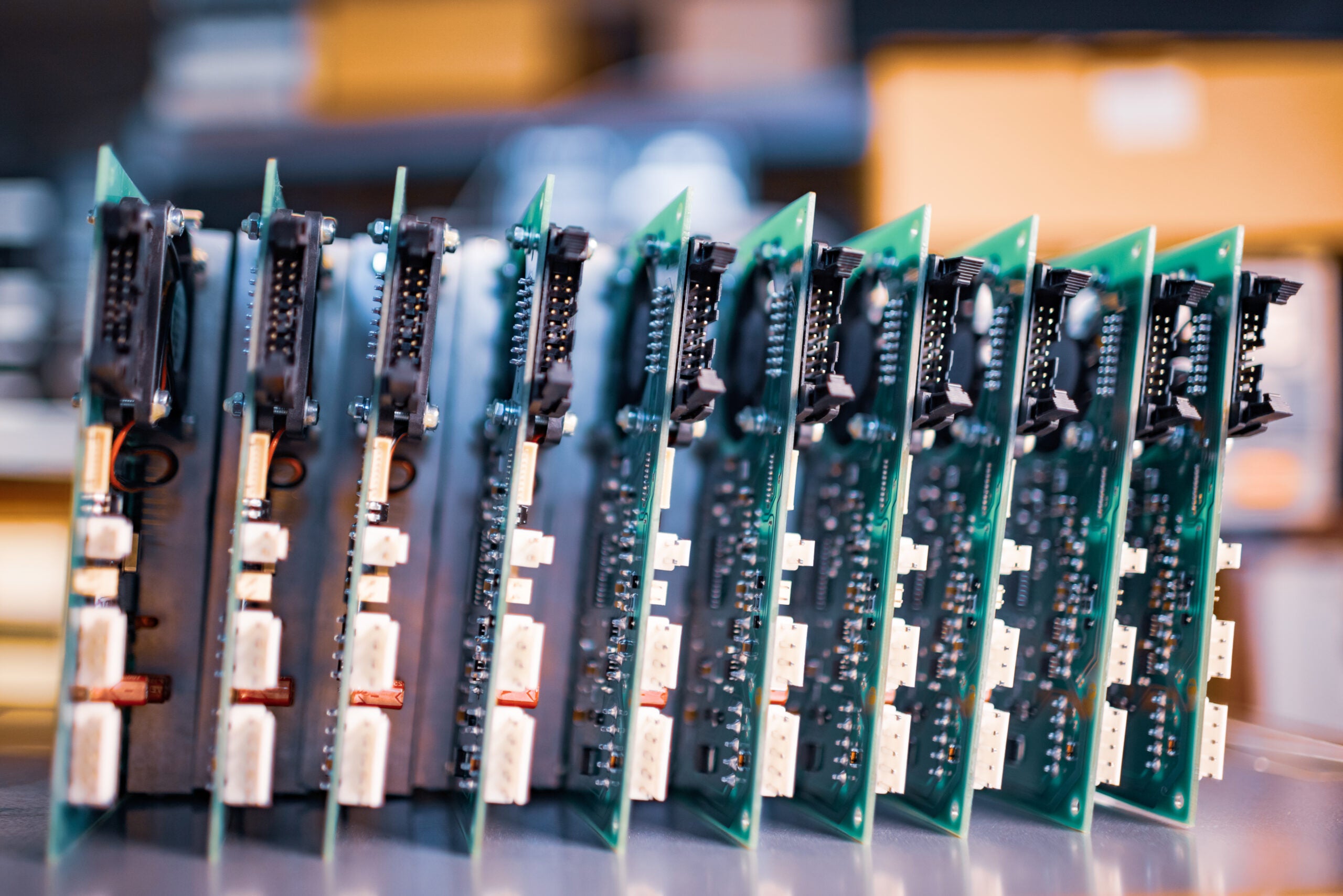
Often, multilayer circuit boards are designed with consistent dielectric layers to maintain a fixed impedance. However, there are cases where performance is improved by taking a heterogeneous approach to PCB stackup design, where the material and/or size of individual layers vary. This approach enables designers to meet demanding requirements for RF applications, high-speed digital circuits, and complex mixed-signal systems while maintaining manufacturing feasibility and cost-effectiveness. Understanding hybrid stackup PCB design principles and optimization techniques is essential for modern PCB designers who face increasingly complex signal integrity, thermal management, and performance requirements across diverse applications.
Step-by-Step Hybrid Stackup PCB Best Practices
Implementing stackup design principles is essential for all multilayer PCB designs. However, optimizing a hybrid stackup design requires these and other considerations, which are included among the steps below:
| Hybrid Stackup PCB Optimization Steps | ||
| Step | Process | Key Considerations |
| 1. Requirements Analysis | Define electrical, thermal, and mechanical requirements | Signal frequency ranges, power levels, and environmental conditions |
| 2. Material Selection | Choose dielectric materials per layer function | Match Dk/Df to signal requirements, consider CTE compatibility |
| 3. Layer Stack Planning | Arrange layers for optimal signal integrity | Place critical signals adjacent to reference planes |
| 4. Impedance Calculation | Calculate controlled impedance for each layer | Account for different dielectric properties per layer |
| 5. Via Structure Design | Plan via transitions between different materials | Consider impedance discontinuities at material interfaces |
| 6. Thermal Analysis | Analyze CTE mismatches and thermal stress | Simulate thermal cycling effects on reliability |
| 7. Manufacturing Review | Validate fabrication feasibility with the supplier | Confirm material availability and process compatibility |
| 8. Simulation Validation | Run SI/PI/thermal simulations | Validate performance before prototype fabrication |
| 9. Prototype Testing | Fabricate and test prototype boards | Measure electrical performance vs. simulation |
| 10. Design Optimization | Refine stackup based on test results | Iterate material selection and layer arrangement |
Following the steps above will help you achieve a PCB stackup where each layer is optimized based on signal type, performance requirements, and the overall design is developed for efficient manufacturing and reliable operation. There are several advantages to adopting this hybrid design approach, yet it is essential to understand the challenges to create your best design, as we will see next.
Advantages and Challenges of Hybrid Stackups
Advantages:
- Cost Optimization: Hybrid stackups deliver significant cost savings compared to all-high-performance material boards. By using premium materials only where needed, designers can achieve 40-60% cost reduction while maintaining critical performance specifications.Â
Â
- Enhanced Signal Integrity: Strategic material placement enables superior signal integrity across multiple frequency bands. RF sections benefit from low-loss materials, while digital sections use materials optimized for controlled impedance and crosstalk reduction.
Â
- Superior Thermal Management: Different materials can be selected based on thermal conductivity requirements. High-power areas can utilize materials with better thermal dissipation, while low-power sections use standard materials, optimizing overall thermal performance.
Â
- Application-Specific Optimization: Each layer can be optimized for its specific function, RF transmission, power distribution, or digital signaling, rather than compromising with a single material across all layers.
Â
Challenges:
- Material Availability Constraints: Specialty RF materials often have longer lead times and limited availability compared to standard FR4. This can impact project schedules and requires early material procurement planning.
Â
- CTE Mismatch Effects: Coefficient of thermal expansion (CTE) mismatches can cause reliability issues at material interfaces and via connections.
Â
- Complex Via Design Requirements: Vias transitioning between different dielectric materials face impedance discontinuities and potential reliability challenges. Via design becomes more complex, requiring careful simulation and optimization.
Â
- Manufacturing Complexity: Hybrid stackups require more sophisticated manufacturing processes, specialized equipment, and tighter process controls.Â
Â
- Increased Design Time: The complexity of managing multiple materials, calculating impedances across different dielectrics, and optimizing performance requires additional design and simulation time.
As shown above, a hybrid stackup PCB design can yield a better-performing board, provided the challenges are overcome.Â
Overcoming Hybrid PCB Stackup Design Challenges
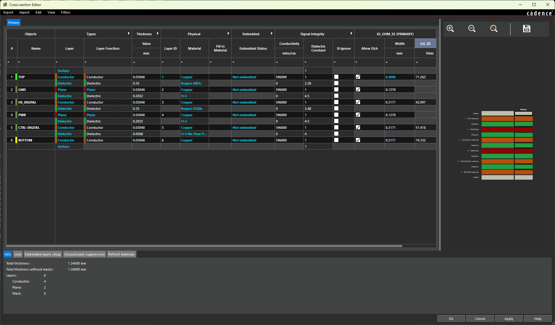
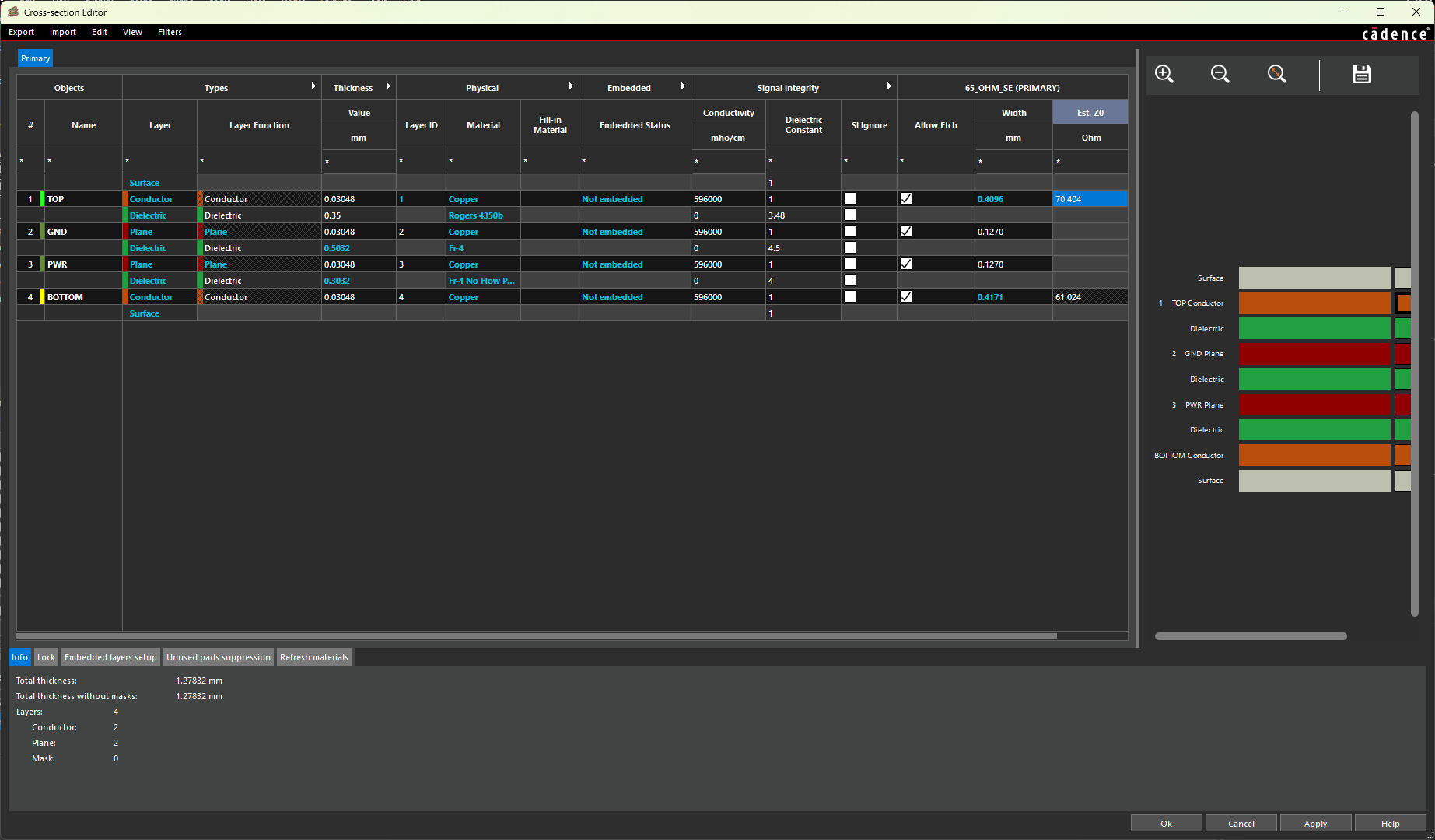
Formulating an actionable plan to optimize your board design with a hybrid stackup requires careful consideration of the best PCB materials for each layer. Below are examples for common 4 and 6-layer stackups.
Standard 4-Layer StackupÂ

Hybrid 4-Layer Stackup

Hybrid 6-Layer Stackup

| Standard vs Hybrid Stackup PCB Examples | ||
| Standard 4-Layer Stackup | Hybrid 4-Layer Stackup | Hybrid 6-Layer Stackup |
|
|
|
The examples above are representative of the options you have to optimize your RF design by employing a hybrid stackup PCB approach. However, it is essential to understand the challenges and prioritize PCB material selection to realize the advantages of this design strategy. Another critical implementation to optimize your design⇒build⇒test (DBT) for minimal spins and high yield is to perform simulations to validate your design before manufacturing.Â
Hybrid Stackup PCB Validation
Hybrid stackup designs demand comprehensive simulation validation before fabrication due to their complexity and cost implications. The interaction between different materials creates unique challenges that cannot be adequately predicted without proper modeling. Types of simulation to perform include:
Running SI simulations is essential for validating impedance control across material transitions, minimizing reflections at via interfaces, and ensuring signal quality across all frequency ranges. Pay particular attention to via transitions between different dielectric materials where impedance discontinuities are most likely to occur.
Power distribution networks in hybrid stackups require careful analysis due to varying dielectric properties across layers. Simulate PDN impedance, validate the effectiveness of decoupling capacitors, and ensure that power delivery meets requirements across all functional blocks.
The material interfaces in hybrid stackups can create unexpected EMI behavior. 3D electromagnetic simulation helps identify potential radiation sources and ensures EMC compliance before fabrication.
CTE mismatches and varying thermal properties necessitate thermal stress analysis. Model thermal cycling effects, validate reliability under operating conditions, and identify potential failure points at material interfaces.Â
Applying modern tools to perform the simulations and analyses listed will ensure you create a design that optimizes performance while minimizing development risks.
