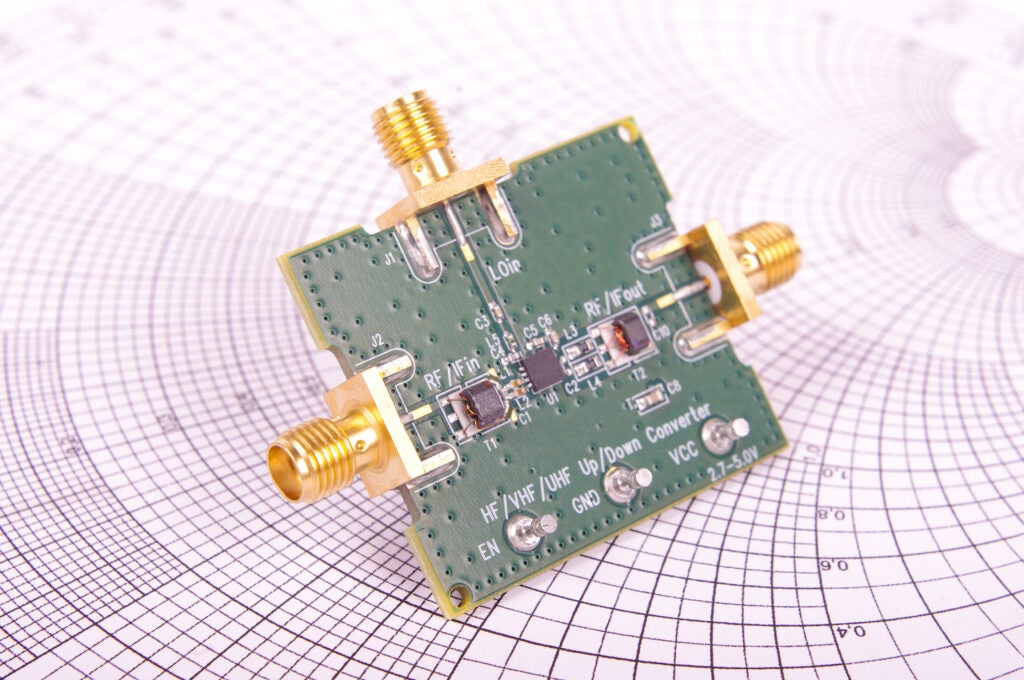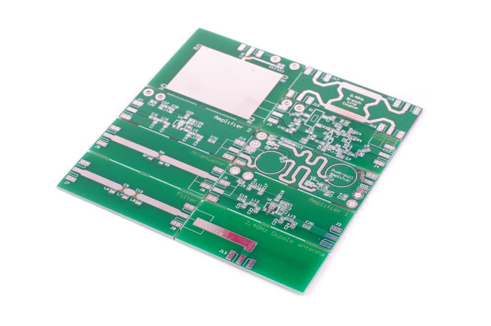
RF designs come with additional challenges and complexities that must be addressed. To create a functional RF design, best RF design layout practices should be followed. Best RF design layout practices include:
- Designing hybrid stack-ups
- Selecting the right PCB materials
- Performing impedance matching
- Designing RF traces
- Optimizing the PDN design
- Incorporating stitching vias
- Placing and routing decoupling capacitors
Implementing RF Design best practices will help to improve performance, achieve better signal isolation, and easily integrate analog and digital circuitry, RF components, sensors, and microcontrollers. The experts at Sierra Circuits and EMA Design Automation will walk you through best practices for RF design layout and provide in-depth knowledge and detailed demonstrations on how to design and analyze your RF PCBs with AWR.
In this webinar, you will learn the best RF design layout practices, including:
- 5 design tips to build an efficient hybrid stackup
- Suitable materials for a hybrid stackup
- Bonding materials used for hybrid stackups
- 4 fabrication challenges in building hybrid stackups
- How Sierra Circuits can help you create reliable hybrid stackups
- How the AWR design environment allows you to design and analyze your RF designs
- Tips to achieve the best RF trace design
- Types of transmission lines
- Tips for power and ground planes in your RF designs
- How to incorporate stitching vias in your RF designs
- Tips for incorporating and routing decoupling capacitors