Today’s fast-paced product development requires efficient techniques to reuse and modify known-good designs. When product revisions are required, design modifications may be necessary due to obsolete components, upgrading technology, or improving circuit performance. OrCAD X allows you to cut traces and reuse parts of a design efficiently with the ability to:
- Update or replace sections of the design
- Reuse known-good circuitry and leverage IP
- Reorganize and move groups of circuitry
This quick how-to will provide step-by-step instructions on how to cut traces to reuse parts of a design in OrCAD X Presto Professional.
To follow along, download the provided files above the table of contents.
How-To Video
 Open in New Window
Cut Traces to Reuse Parts of a Design
Step 1: Open the provided board in OrCAD X Presto Professional 24.1. For this example, we will replace the main USB connector on the board with a newer USB-B 3.0 connector. The original connector has already been removed.
Note: The ability to cut traces is a new feature in the 24.1 release. For more information about new features in OrCAD X, get a full version history here.
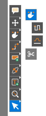
Step 2: Right-click the Slide mode in the toolbar and select Cut Traces.
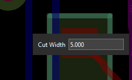
Step 3: The Cut Traces mode is activated. In the Cut Traces widget, adjust the cut width to 5.
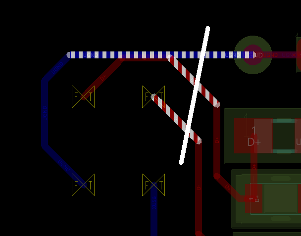
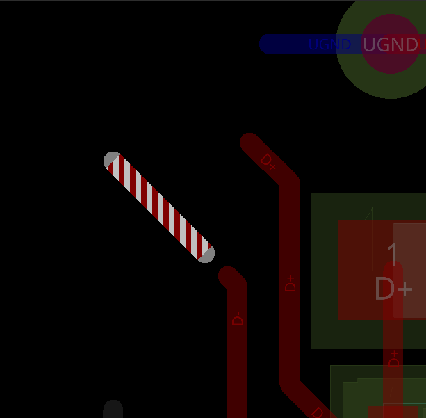
Step 4: Click to start drawing the cut line across the traces UGND, D+, and D- which connected to the original USB connector. Click again to finish. The traces are cut.
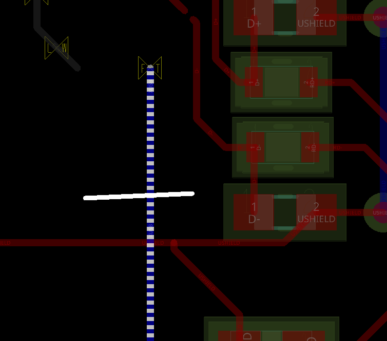
Step 5: Click to draw a cut line across the XUSB trace. Click again to finish. The free section of trace is reassigned to the GND net.
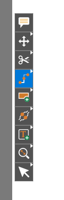
Step 6: Choose the Select mode from the toolbar.
Step 7: In the Properties panel, in the Selection Filter subpanel, select Trace Segments and Nets to remove them from the selection filter. This will make individual traces easier to select.
Step 8: Select the free trace sections and press Delete on the keyboard to remove them.
Step 9: Select File > Save from the menu. Click Yes when prompted to overwrite the design.
Updating Components in a PCB Design
Note: For this example, technology changes have already been made in the schematic and synced to the PCB design. If the schematic file is available, select ECO > Update PCB from the menu to sync the PCB to the schematic.
Step 10: Select ECO > Quickplace Components from the menu.
Step 11: USB connector J12 is placed above the PCB design. Select the Move mode from the toolbar to adjust it.
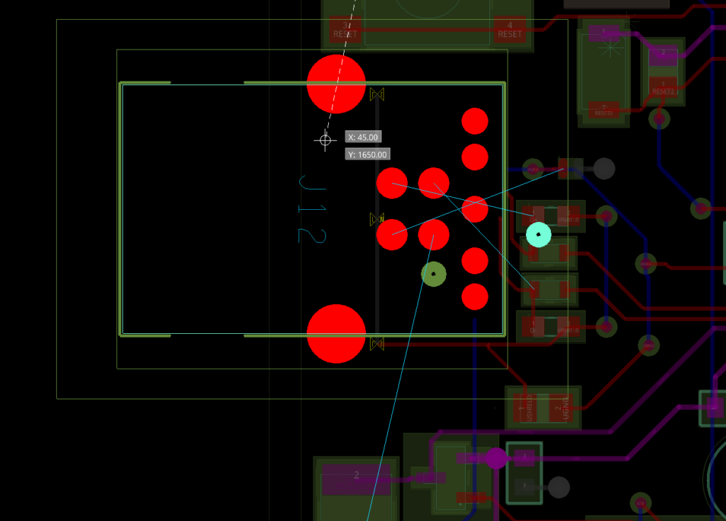
Step 12: Click to attach the connector to your cursor. Move the connector to the empty spot on the board. Press R to rotate such that all pads are facing the board. Click again to place the connector.
Step 13: Choose the Select mode from the toolbar or press Escape on the keyboard to end the Move mode. Click in the blank canvas to deselect the shape.
Step 14: In the Properties panel, select the X for Shape Islands to clear any newly-created shape islands.
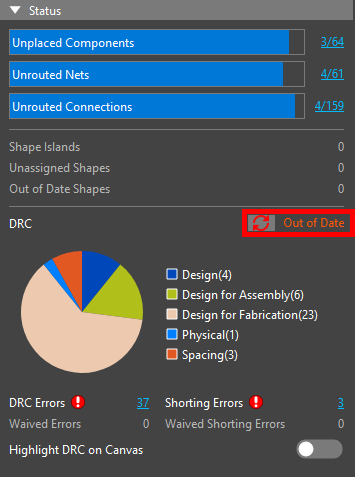
Step 15: Select Refresh to update the DRC cache.
Completing the PCB Layout and Routing
Step 16: Select Trace Segments in the Selection Filter subpanel to re-enable trace segment selection.
Step 17: Select the Add Connect mode from the toolbar to re-add the connections.
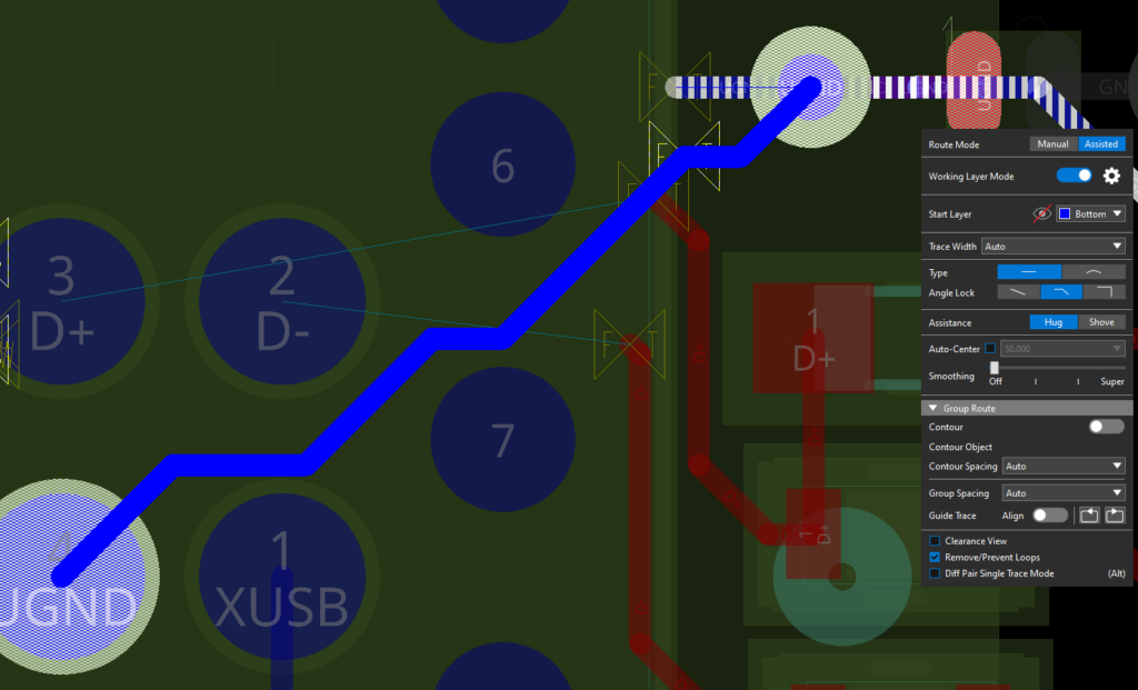
Step 18: Click to start routing traces from the pins of the new connector to the remaining trace connections. Use the ratsnest lines to determine the original connections. Click the end of the ratsnest line to finish.
Note: To shorten existing traces, use the Slide mode to smooth the trace or select the unnecessary segments and press Delete on the keyboard.
Double-click or press V on the keyboard to add vias as needed.
In the Add Connect widget, select Assisted for the Route Mode to avoid creating additional DRC errors.
Check Diff Pair Single Trace Mode to route D+ and D- around the unconnected high-speed pins easier.
Step 19: When the port is reconnected, choose the Select mode from the toolbar.
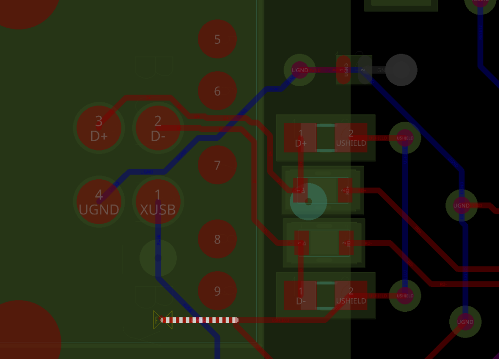
Step 20: Click to select any remaining stray vias or traces and press Delete on the keyboard.
Wrap Up & Next Steps
Efficiently cut traces to reuse parts of a design or replace specific circuitry with OrCAD X Presto to accelerate the PCB design process. Test this feature and more with a free trial of OrCAD. For more how-tos and step-by-step walkthroughs, visit EMA Academy.

