Switching ECAD tools mid-project, or mid-career, is one of the highest-friction decisions an engineering team makes. Get the data migration right, and you carry forward years of design intellectual property (IP). Get it wrong, and you’re manually rebuilding netlists and footprint libraries for weeks.
OrCAD X includes an integrated Altium Designer translator, enabling you to migrate from Altium to OrCAD without third-party middleware on standard boards. This guide walks through the exact, native workflow, including file preparation through post-translation library extraction, so you can land in OrCAD X with a clean, synchronized design.
Before touching any import utilities, understand how Altium’s file types map to OrCAD’s environment:
| Altium File / Concept | OrCAD Equivalent | Notes |
| .SchDoc (ASCII) | .DSN | Core schematic design file |
| .PcbDoc (ASCII) | .BRD</span< | Physical PCB layout database |
| Project Master (.PrjPCB) | .OPJ | Top-level project file |
| .PrjPCBStructure | (Translator Input Only) | Encodes multi-sheet hierarchy |
| Component Properties | Property Editor | Stores MPN, Value, Tolerance |
| .SchLib | .OLB (Capture) | Native OrCAD symbol library container |
Phase 1: Preparing Files for Export to Migrate from Altium to OrCAD
The Cadence translation engine requires cleanly structured, ASCII-formatted data. The schematic must be saved to ASCII format within Altium Designer. This replaces the original binary file with its ASCII equivalent, while the location and file extension stay the same. Binary Altium files cannot be read directly by OrCAD import utilities.
Your Altium Designer schematic data can be translated only if it is embedded in a PCB project (.PrjPCB), which manages the design documents required to manufacture a PCB. Skipping this preparation phase is the leading cause of broken netlists during migration.
Execute these steps inside Altium Designer before touching OrCAD:
- Save as ASCII: Open each schematic (.SchDoc) and PCB layout (.PcbDoc) file, then use File > Save As and select the ASCII format option. The file extension stays the same, and only the encoding changes.
- House in a PCB Project: Your Altium Designer schematic files can be translated only when embedded in a PCB project (.PrjPCB). Verify all design documents are correctly linked inside the project file.
- Generate the Structure File: Compile the PCB project in Altium. A valid structure file (.PrjPCBStructure) is needed, and it is generated after compiling the PCB project and references the individual schematic pages (.SchDoc). Without it, OrCAD cannot reconstruct how your multi-sheet or hierarchical pages connect.
Phase 2: The Core Translation Process
Translation happens in two distinct stages: schematic import and layout import. Both utilities are native to the OrCAD X suite.
Translating Schematics into OrCAD X Capture
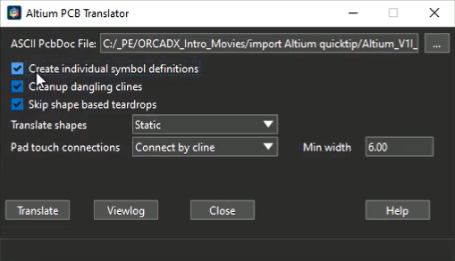
The schematic translator parses your ASCII .PrjPCB file and reconstructs logic, page sizing, and symbols inside OrCAD Capture. Always output to an empty directory, as writing into an existing OrCAD project folder will cause file conflicts.
In OrCAD X Capture, click File > Import > Altium Schematic Translator to launch the Altium-Capture translator. Browse to the ASCII.PrjPcb file and specify the output directory for the OrCAD X Capture project.
Additional translator options worth knowing:
- Frame Size: Sets the sheet size and layout for translated schematic sheets. Standard ANSI and ISO sizes are supported.
- Library Optimization: When “Create Individual Symbol Definitions” is checked, the translator generates a separate symbol definition for each component instance by adding a suffix to the component’s name. For example, 0805_1, 0805_2, 0805_3, to account for instance-specific footprint modifications.
Once the status window confirms success, click “Viewlog” to review the translation log for any errors or warnings before proceeding. Close the translator. The translator will have generated a .DSN file in your specified output directory (the .OPJ project file does not yet exist and must be created separately). In OrCAD X Capture, select .File > Open > Design, browse to the generated .DSN file, and click Open. A prompt will appear to define the project name and location. Click OK to generate the .OPJ and open the project. Verify that all schematic pages and hierarchical blocks populated correctly.
Importing the Altium PCB Layout
The physical board translation rebuilds your stackup, traces, polygons, and footprints inside OrCAD X.
Open a blank layout in OrCAD X, then select File > Import > Altium PCB from the menu. From there:
- Browse to your exported ASCII .PcbDoc file.
- Check “Create Individual Symbol Definitions” to prevent footprint collision errors when instance-level modifications exist on the board.
- Note the “Skip Shape Based Teardrops” option: Altium generates teardrop traces from shapes and tracks, but teardrops in OrCAD X are parameter-driven rather than shape-derived, so this option is worth enabling for cleaner output.
- When the translation and import finish, the board design opens in the OrCAD X canvas. Review the design and correct errors as needed.
- The translated PCB layout appears in the main editor window. Save the .BRD file (it will be found in the same location as the original Altium.pcbdoc.file) before continuing.
Phase 3: Post-Migration Cleanup and Library Management
No EDA translation is perfect. Non-standard graphical shapes, custom text formatting, and complex multi-sheet hierarchies may require manual intervention. Your immediate priorities post-translation are library extraction and netlist synchronization.
OrCAD uses a different database architecture than Altium. Rather than standalone .SchLib files, the translated design stores all components in a local Design Cache. You need to pull those cached symbols into a formal library file before they’re usable across other projects.
In OrCAD X Capture, navigate to the Project Hierarchy and find the Design Cache under the Design File Folder. This cache contains one instance of every schematic symbol used in the design.
Follow these cleanup steps:
- Extract the Library: Select all parts in the Design Cache, then Copy and Paste them into a new Library file (File > New > Library). This produces a .OLB file that becomes your native OrCAD symbol library for future reuse.
- Normalize Attributes: Select the top-level schematic root and open Edit Object Properties. The Property Editor matrix appears; you can copy all cells (Ctrl+C), paste them into Excel, normalize attributes like MPN, Tolerance, and Voltage Rating in bulk, then paste the cleaned data back into OrCAD.
- Check Net Naming: Non-aliased nets may revert to an OrCAD default naming style during translation, something like N00027 instead of a meaningful signal name. Audit net names in the schematic before pushing the netlist to layout.
- Watch for Signal Harnesses: Altium’s signal harness construct has no direct equivalent in OrCAD Capture. Designs using harnesses heavily should be reviewed manually before netlisting. Harness-bundled nets may need to be re-expressed as standard OrCAD buses or off-page connectors.
- Synchronize the Netlist: Run a DRC on the schematic. Once it passes, select PCB > Update Layout in OrCAD X Capture to push the logical connectivity to your translated .BRD file.
- Review the Log File: Ater schematic translation is complete, click “Viewlog” in the Altium Schematic Translator and review the log for errors before proceeding.
Ready to upgrade your design workflow? Now that you know how to successfully migrate from Altium to OrCAD, it’s time to test the waters with your own files. OrCAD X comes equipped with built-in translators for the most popular EDA applications, ensuring a smooth transition without sacrificing your legacy IP. If your team is evaluating the switch, contact EMA Design Automation for a migration consultation and trial access to OrCAD X. Their step-by-step how-to guides for both schematic and PCB import are among the most detailed available outside of Cadence’s own documentation.
EMA Design Automation is a leading provider of the resources that engineers rely on to accelerate innovation. We provide solutions that include PCB design and analysis packages, custom integration software, engineering expertise, and a comprehensive academy of learning and training materials, which enable you to create more efficiently.
For more information on how to migrate from Altium to OrCAD and how we can help you or your team innovate faster, contact us.