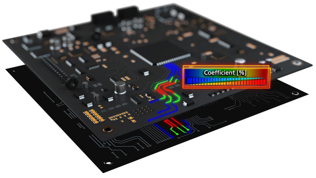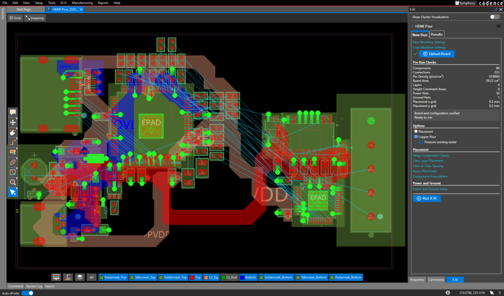
Artificial Intelligence (AI) has been the buzz word across all industries, and not surprisingly, a hot topic in PCB design. AI can be used to accelerate the PCB design process, from schematic and block diagram creation with tools like Circuit Mind to component placement and automatic copper pours with Allegro XAI. Regardless of what tools you’re using to leverage AI for PCB layout, it is essential to define the correct settings and configurations for maximum impact and best results.
Use Cases of AI for PCB Layout
In today’s engineering environments, AI is starting to make a big impact on PCB layout as it can handle optimization, automation, and prediction tasks that are often time-consuming or complex for designers. AI is often used as a jump start to the PCB layout and has the following use cases:
- Initial Component Placement
- Initial Design of Metal Pours
- Initial Board Routing
- Signal integrity and power integrity predictions
- Thermal management optimization
- Incremental flows for ECO scenarios
- Evaluation of trade-off decisions
- Fitment and feasibility studies
- Optimize layer stackups
- Optimize board outlines
While the quality and accuracy of AI for PCB layout is still evolving, you can increase AI success with three simple steps.
Step 1: Define Design Intent (AI Hints)
Providing detailed design information gives the AI a framework, or a set of guidelines, that directs how it evaluates trade-off decisions and optimizes the PCB layout. Critical design information should be defined within your PCB tools upfront to assist AI in determining the rules and constraints which must be followed when attempting to place components, design power planes, or route the board. Without this context, results may be technically correct but misaligned with your priorities. The schematic and PCB should be configured with the important information to produce the best AI outcomes, including:
- Electrical Functionality
Electrical functionality should be defined upfront in the schematic to ensure proper component placement, copper pours, and routing. During the schematic, take the following actions to improve the performance of AI for PCB layout:
-
- Use industry-standard reference designators
- Connect all nets
- Define voltage requirements
- Group components by electrical functionality into rooms
- Configure critical nets such as differential pairs
- Critical Rules
Define the constraints for the design which will affect functionality and manufacturability. Rules should be configured for:
-
- Physical elements in the PCB layout, such as minimum line width, allowed vias, minimum blind/buried via stagger, etc.
- Differential pairs including minimum line spacing, primary gap, and neck gap
- Spacing between objects in the design and critical elements, such as lines, shapes, pins, holes, vias, and test points.
- Primary routing layers for nets in the design
- Manufacturing requirements
- Component Classifications
Define the reference designators used for each component class such as ICs, discretes, and connectors. Component classes can be used to create logical groups and set constraints during the placement process. Classifying components enables you to define the following:
-
- Clearances between component classes
- Side of the board for component placement based on the part type
- Power and Ground
Define and/or verify the power delivery network including the pin count for the design, voltage requirements, and current requirements. Additionally, ensure all nets which have a DC voltage are assigned to a specific layer in the design. If using AI tools to design the copper pours in the PCB layout, make sure to define if nets should fill the entire layer or if the layer can be mixed (containing both poured shapes and signal routes). Be sure to specify the PCB layers in the stackup on which each power and ground net should or should not be poured.
The following table summarizes the settings which should be configured to improve AI results.
Essential Design Settings and Configurations for AI-Enhanced PCB Layout
| AI Inputs | Requirement | Purpose | AI Application |
|---|---|---|---|
| Reference Designators | Consistent reference designators per component class. | Provides understanding as to what components are. |
|
| Voltage Nets | Voltage levels for each net in the design. | Helps define power and ground requirements. |
|
| Functionality Groups | Logical groups of functional component blocks in rooms. | Enables close placement of critical parts and their supportive circuitry. |
|
| Physical Rules | Physical rules for nets in the design. | Dictates appropriate trace properties, vias, and more. |
|
| Spacing Rules | Minimum spacing for nets, objects, and parts in the design. | Dictates appropriate trace and component spacing. |
|
| DFM Rules | Rules which conform to your CM’s capabilities. | Increases manufacturability. |
|
| Differential Pairs | Traces included in differential pairs and additional rules. | Guarantees proper operation. |
|
| Routing Requirements | Specific layers for routing nets, power/ground. | Simplifies routing and defines layer priorities. |
|
| Component Classifications | Map component classes & reference designators. | Intelligent placement and spacing of parts. |
|
| Component Clearances | Minimum distance between component classes. | Prevents overlapping pins. |
|
| Component Locations | Preferred board side for each component class. | Reduces manufacturing costs. |
|
| Voltage Layer Assignments | Layers designated for power and ground planes. | Optimizes PDN efficiency and accuracy. |
|
Effectively communicating your design intent is critical to unlocking the full potential of AI in engineering and PCB design. AI is not a replacement for your expertise, but a powerful tool that amplifies it. The more clearly you define your goals, constraints, and preferences, the better the AI system can align its recommendations and actions with your objectives. By articulating your intent, you enable AI to focus on what it is good at.
Step 2: Let AI Focus on What It’s Good At
There is little value in having AI iterate across thousands of potential options when the correct solution is already known. Predefining certain items which are fixed due to design requirements reserves AI resources for areas where flexibility and optimization matter most—such as placement, copper pours, routing, thermal management, or signal integrity—ensuring the greatest efficiency and value. To let AI focus on optimized solutions that best meet your needs, the following methods should be deployed:
- Preset Mechanical Components
Lock critical components, connectors, and mechanical elements that you do not want moved during the PCB layout. Pre-placing and locking these components will provide AI tools with a starting point and ensure any components which are vital to mechanical integration and functionality are placed correctly.
- Route Critical Pre-Defined Paths
Pre-route critical nets and pours to ensure functionality and performance. Lock these paths in place to prevent changes. If you don’t want AI to change elements, be sure to lock them in place to help the AI engine know those pieces are not to be changed and it should work around them.
- Define Rooms on the PCB
If rooms have been defined in the schematic, create room outlines on the PCB. This will ensure components are placed within the constraints of the outline and on the appropriate side of the PCB. If no room outline is defined, AI tools will typically create “floating” rooms, where components are placed together in the best available location.
With these foundational elements locked in, AI tools for PCB layout can concentrate on solving the challenges that truly benefit from optimization; however, even the most advanced AI-generated layouts still require a critical step: review and verification. This ensures the design not only meets electrical and mechanical requirements but also aligns with your overall intent.
Step 3: Review and Verify the Results
AI-assisted PCB design is rarely a one-and-done process; much like current PCB design flows, it works best as an iterative cycle of running the AI, reviewing the results, making adjustments, and running it again. The true measure of success isn’t perfection on the first pass, but the overall time and effort saved compared to a fully manual approach. When AI reduces repetitive work and accelerates key steps, it delivers real value by enhancing both productivity and design quality. The following tips will help you review and verify AI results to get the most out of this powerful new addition to the PCB designer’s toolkit:
- View Any Generated Reports
AI tools typically generate a variety of reports to help designers review, verify, and validate the PCB layout. These reports can include:
-
- Impedance reports
- Signal integrity checks
- Thermal reports
- Timing reports
- Placement and routing summary reports
- Review and Correct Design Rule Errors
AI does its best to conform to the rules and constraints defined within CAD tools but sometimes a solution cannot be found. In these cases, design rule violations will occur. Leverage your CAD tools design rule checking abilities to identify and correct errors before continuing with the PCB layout.
By reviewing reports, correcting rule violations, and refining the AI’s output, designers maintain full control while benefiting from automation.
AI for PCB Layout: Essential AI Configuration Checklist
Configuring essential settings and constraints up front not only minimizes errors but also allows the AI to focus on where it delivers the most value. The following checklist can be leveraged to ensure the necessary settings are configured, producing optimal results when leveraging AI for PCB layout:
Schematic & Design Intent
-
-
- Verify all net connections are complete and correct
- Use consistent reference designators across components
- Define voltage nets and assign correct voltage/current requirements
- Group components into functional rooms for logical placement
- Identify and define critical nets
-
Component & Placement Rules
-
-
- Classify components and map reference designators
- Fix mechanical components
- Define component clearances between classes
- Assign components to preferred board sides
- Create room outlines on the PCB to guide placement
-
Routing & Electrical Rules
-
-
- Define trace width, vias, and stackup rules
- Configure spacing rules for nets, components, and copper features
- Assign differential pairs with appropriate spacing and gap constraints
- Define routing layers for specific nets or classes
- Lock in pre-routed critical nets and pours to preserve them
- Configure the PDN with proper layer assignments
- Specify which PCB layers should be reserved for power and ground
-
Manufacturing & Testability
-
-
- Apply DFM rules from your PCB manufacturer
- Define test points and ensure accessibility for probes
-
By applying this checklist, you establish a solid foundation for AI to operate effectively within your PCB design workflow. With the essentials clearly defined, AI can focus on delivering optimized layouts, improved efficiency, and higher-quality results.
Maximizing the Impact of AI in PCB Design
AI is transforming the way PCB designers approach complex layouts, offering opportunities to accelerate workflows, optimize performance, and explore design alternatives more efficiently than ever before. However, the full benefits of AI can only be realized when designers provide clear guidance and define essential constraints.
The key takeaway: clear intent, proper configuration, and careful review are the pillars of AI-enhanced PCB design, unlocking productivity gains and setting the stage for the next generation of design innovation.
Ultimately, AI is a powerful ally, not a replacement for human expertise. When used as intended, it reduces repetitive tasks, minimizes errors, and frees designers to focus on innovation and higher-level decision-making. As AI tools continue to evolve, integrating them effectively into your PCB workflow will become a standard part of modern design practice, driving faster, smarter, and more reliable designs.