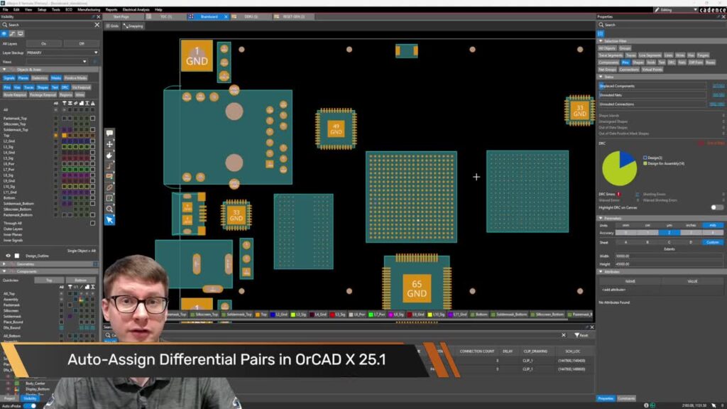
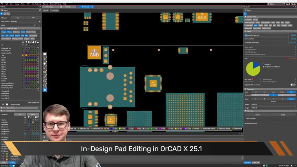
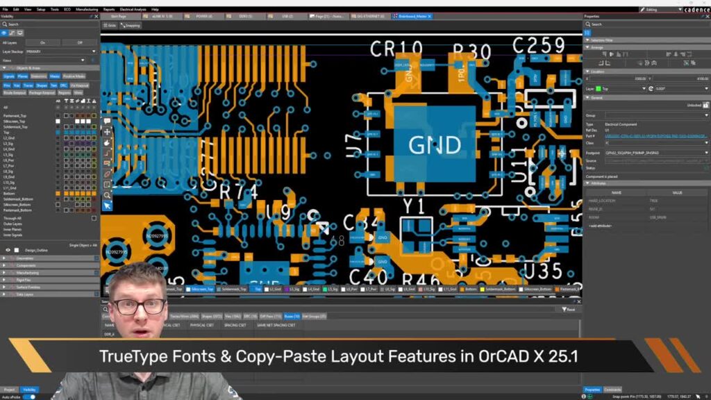
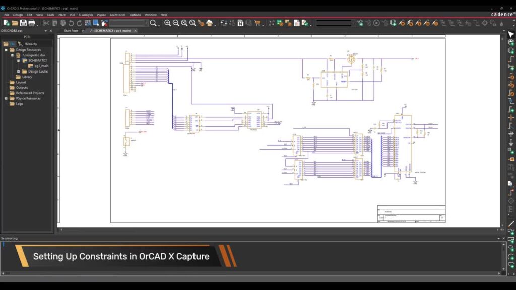
SMD pads are commonly used in PCB footprints. This video will teach you how to create SMD pads in OrCAD PCB Designer 17.4. Throughout this video, you will learn about:
- The user interface and GUI of the Padstack editor in OrCAD and Allegro PCB
- Types of mask layers
- How to create pads for surface mount devices (SMD)
- How to adhere to IPC standards by:
- Determining the margins
- Determining offsets
- Determining naming conventions
- How to use newly created padstack
To view the demo files and follow along, click here.
Learn how to create IPC compliant through-hole padstacks for your PCB footprints here.


