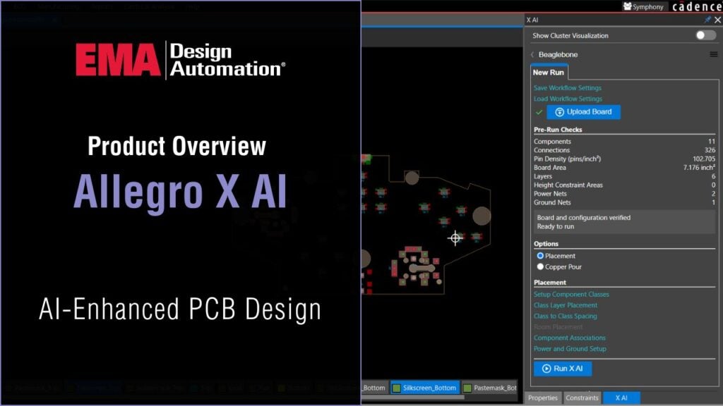
Good signal integrity is vital to the performance of your PCB. Performing pre-layout analysis will help determine and validate critical rules to achieve the desired signal performance. In this video, you will learn how to:
- Identify supply nets
- Define stackups and constraints
- Configure your design for pre-layout analysis
- Use the SI Design Wizard in OrCAD PCB 17.4
This is the first video of this 5-part series:
- PCB SI Basics: Setting Up a Design for Pre-Layout Simulation
- PCB SI Basics: How to Assign IBIS Models and Extract Topology
- PCB SI Basics: Understanding the SigXP User Interface
- PCB SI Basics: Performing Simulation with Lossless Transmission Lines
- PCB SI Basics: Performing Simulation with Lossy Transmission Lines
To view the demo file, click here.