Similar to coupling, crosstalk is a phenomenon that occurs between close conductors transferring energy to each other. Crosstalk can occur in any circuit due to parasitic inductance and capacitance, as well as the changing magnetic field generated when current through a trace or wire changes. Understanding crosstalk, it’s impact on signals, and effective mitigation strategies is especially important for high-speed or fast-edge signals.
What is Crosstalk?
Crosstalk refers to unwanted electromagnetic coupling between adjacent signal traces, which can degrade signal integrity. It typically appears as noise or interference on a “victim” trace due to signals on an adjacent “aggressor” trace. Crosstalk can occur due to capacitive or inductive coupling:
Capacitive Coupling
Capacitive coupling occurs when two conductors are close enough that the electric field from one induces a voltage in the other. This is common in closely spaced traces or between traces and ground planes.
Inductive Coupling
Inductive coupling occurs when a changing magnetic field induces a current in an adjacent trace or loop. This is commonly seen in tightly coupled loop areas or power traces for high-speed signals and power lines.
Regardless of which type of crosstalk your design may be exhibiting, it is important to be aware of these effects, understand how to measure the impact, and assess mitigation strategies if needed.
How to Measure Crosstalk
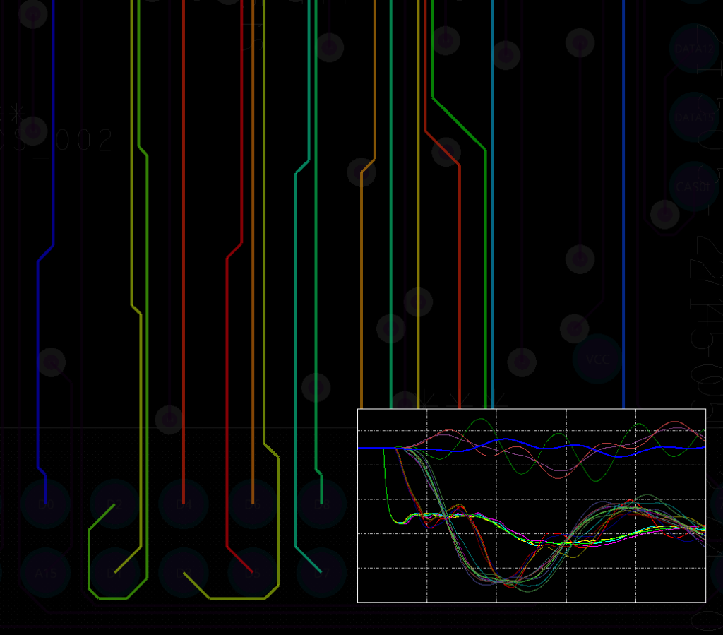
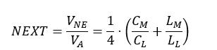
Crosstalk is typically measured as a noise voltage peak or a plotted curve. To measure crosstalk, calculations should consider coupling with evaluation of the coupling coefficient as it is a significant contributor to crosstalk. The coupling coefficient is used to express the strength of all induced coupling on a given trace. Coupling coefficient for a trace is dependent on its per-unit near-end crosstalk, or NEXT.
Step 1: Calculate Near End Crosstalk
Near-end crosstalk is calculated by the following formula:
Where:
VNE = Near End Voltage
VA = Aggressor Voltage
CM = Mutual Capacitance
CL = Victim Line Capacitance
LM = Mutual Inductance
LL = Victim Line Inductance
Step 2: Calculate the Saturation Length
Signal rise time also needs to be considered for the coupling coefficient. A saturation length is calculated from:
Where:
Tr = Rise Time
Vs = Signal Velocity
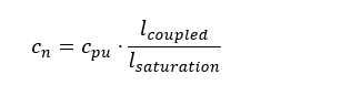
Step 3: Determining the Coupling Coefficient
From there, the coupling coefficient of a pair of traces is calculated as follows.
If the coupled length is greater than or equal to the saturation length, the coupling coefficient is the same as the NEXT coefficient.
If the coupled length, lcoupled, is less than the saturation length, the coupling coefficient is calculated by:
Where:
cn = Total Coupling Coefficient
cpu = NEXT Coupling Coefficient
Once we are able to effectively calculate the crosstalk, we can then begin to assess its impact and identify causation.
Understanding the Impacts from Crosstalk
Crosstalk can affect overall system performance and have several negative effects on signal quality including the following common signal integrity issues:
- Signal Degradation
Unwanted noise on a victim trace can distort the original signal shape leading to voltage margin reduction, timing errors, and/or data corruption.
- False Triggering
In analog of mixed-signal circuits, crosstalk can cause false triggering in devices such as comparators and analog-to-digital converters. This can result in incorrect measurements and behavior.
- Jitter
Crosstalk can cause timing uncertainty or jitter, making clock and data edges appear at slightly varying times.
- Cumulative Noise
Crosstalk can add up from multiple aggressors, especially in large buses and arrays common in parallel memory buses like DDR. This creates a higher noise floor and makes the design more prone to errors.
- Increased EMI
Crosstalk can increase the overall radiated emissions and can lead to failure during testing for EMI and regulatory compliance.
- Bit Rate Errors
In high-speed designs, crosstalk can affect signal transitions across thresholds and result in the interpretation of incorrect data and increased bit rate errors.
To prevent these issues, PCB designers must try to minimize crosstalk through mitigation strategies.
Common Causes of Crosstalk
Crosstalk can arise from various factors throughout the PCB layout. The table below will help to identify the cause of crosstalk, why the PCB feature induces crosstalk, and a solution to help PCB designers identify and correct crosstalk.
| Cause | Problem | Solution |
|---|---|---|
| Close Proximity of Traces | Traces routed too closely together allow the electric and magnetic fields from one trace to couple into another. | Increase trace spacing. |
| Parallel Routing Over Long Distances | The longer the parallel trace segment, the greater opportunity for signal energy to couple. | Develop a routing strategy. |
| Inadequate Layer Stackup | Using an improper stackup with multiple signal layers next to each other without isolation can increase crosstalk. | Optimize the layer stackup and incorporate ground shielding. |
| Impedance Discontinuities | Impedance mismatches can cause reflections which can radiate additional fields and couple to nearby traces. | Implement controlled impedance. |
| Inconsistent Differential Pair Routing | Poor control of the spacing between differential pairs or between the pair and nearby signals can lead to crosstalk. | Use differential signaling. |
| Non-Orthogonal Routing on Adjacent Layers | Parallel traces on adjacent layers can result in broadside crosstalk. | Develop a routing strategy and optimize the layer stackup. |
Mitigation Strategies for Crosstalk
Crosstalk must be addressed to improve signal quality in your PCB designs, ideally throughout the PCB design process when change is easiest to implement. To minimize crosstalk, the following strategies can be utilized:
1. Increase Trace Spacing
The primary cause of crosstalk is the proximity of traces. Increase spacing between high-speed or sensitive signal traces to reduce crosstalk and coupling. A good rule of thumb is to increase trace spacing to be 3x the trace width distance between the victim and aggressor traces.
- Increase Separation Between Sensitive Traces
- Implement Trace Spacing 3x the Trace Width Distance
2. Implement Controlled Impedance
Ensure traces are designed with controlled impedance to match the source and load. Many software packages will allow you to configure rules for impedance and automatically check adherence to those rules throughout the PCB layout. If needed, use termination resistors, such as series or parallel termination, to match the impedance and absorb reflection as reflected signals from unterminated traces can lead to resonance and increased radiation increasing crosstalk.
- Design for Controlled Impedance
- Include Proper Termination
3. Optimize Your Grounding Strategy
Incorporating ground shielding will isolate sensitive traces and minimize crosstalk. Optimize your ground strategy by implementing solid ground planes to provide a low-impedance return path and shield traces from each other. Additionally, place ground or power traces between signal traces to act as shields and reduce crosstalk.
- Use Solid Ground and Power Planes
- Isolate Sensitive Signals
4. Optimize Differential Signaling
Using differential pairs for high-speed signals can improve noise immunity and reduce crosstalk. Keep differential pairs tightly coupled to minimize external noise. Utilize software features to ensure proper differential signaling such as rules or constraints to configure differential pairs. Constraining differential pairs will ensure signals remain balanced and noise canceling remains effective by configuring parameters including line width, primary gap, neck width, neck gap, gather control, maximum uncoupled length, tolerance, and more.
- Implement Differential Signaling
- Define Rules to Ensure Tight Coupling
5. Develop a Routing Strategy
Developing a routing strategy for your PCB design can help minimize crosstalk. Within this routing strategy, it is important to minimize parallel routing between sensitive traces and traces on adjacent layers. Additionally, high-speed or noisy signals should be routed far from sensitive signals or even on differing layers in the PCB design. Keep connections short to minimize the likelihood of crosstalk.
- Route High-Speed and Sensitive Signals on Different Layers
- Keep Connections Short
- Avoid Routing Sensitive Traces in Parallel
- Route Traces on Adjacent Layers Orthogonally
Implementing these mitigation strategies throughout the PCB design process can result in many benefits and allow you to set the design up for success. But identifying the crosstalk issues may be difficult and time-consuming. How do you know when and where to deploy these mitigation strategies?
Incorporating Simulation
To identify where additional mitigation is needed in your PCB design, simulation can be deployed to quickly pinpoint crosstalk. Simulation tools typically calculate and analyze crosstalk based on the trace layout, stack-up, and material properties. Simulation can be used to analyze signal integrity and identify crosstalk created by:
- Trace proximity
- Parallel trace routing
- Impedance discontinuities
Once these issues are identified, mitigation strategies can be incorporated into the PCB design to reduce crosstalk and, in turn, improve signal integrity.
Why Should You Analyze Crosstalk?
Implementing mitigation strategies for crosstalk and performing crosstalk analysis not only improves the performance of your PCB designs but also helps you adhere to the project requirements and timeline. Performing crosstalk analysis can benefit your PBC design process by:
- Improving Signal Quality
Performing crosstalk analysis will minimize crosstalk and improve common signal integrity issues including:
- Distortion: Crosstalk can distort the original signal and cause errors in data transmission.
- Noise Induction: Unwanted noise from adjacent signals can corrupt the intended signal and reduce the signal-to-noise ratio (SNR).
- Improving Timing and Data Quality
Analyzing and reducing crosstalk can ensure proper timing and improve the quality of data by minimizing:
- Bit Errors: Crosstalk can lead to bit errors where the signal is incorrectly interpreted.
- Data Corruption: Crosstalk-induced noise can corrupt transmitted data and lead to unreliable communication or system failure.
- Jitter: Crosstalk can introduce timing variations and affect the synchronization of digital signals.
- Signal Skew: Crosstalk can cause variations in signal arrival time, resulting in skew between signals and affecting performance.
- Reducing Electromagnetic Interference
Crosstalk can contribute to increased electromagnetic emissions and lead to non-compliance with EMI regulations. Analyzing and improving crosstalk can help guarantee compliance with industry standards during the design.
Performing crosstalk analysis at any stage of the design is going to have benefits but having this as the last step in your design process can result in late-stage design changes, additional rework, and more design hours if any issues are found. Analyzing crosstalk throughout the PCB layout will allow you to find and correct impedance discontinuities while you are designing- this is where Sigrity Aurora can help.
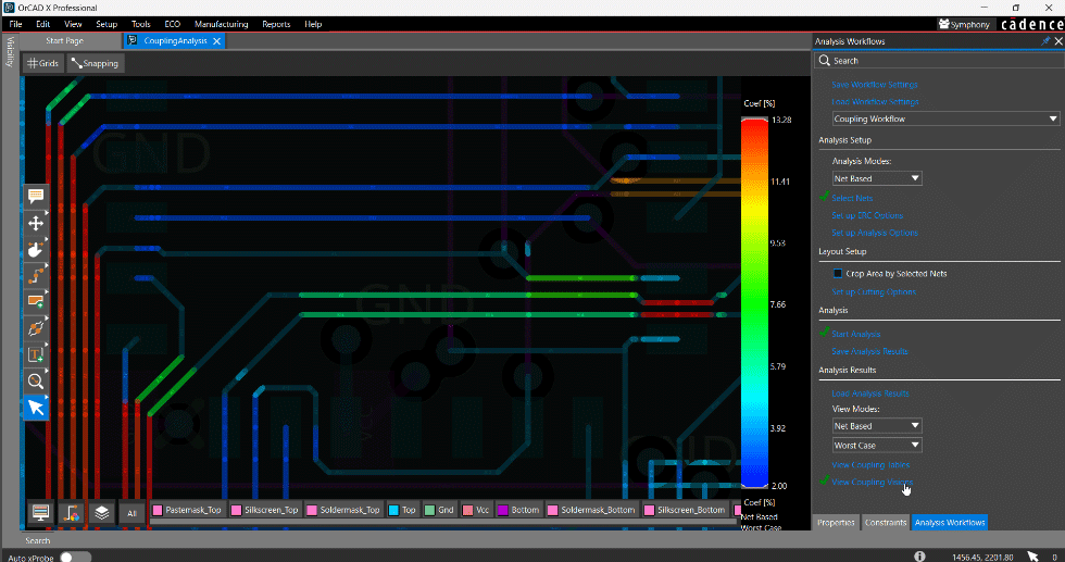
Analyzing Crosstalk with Sigrity
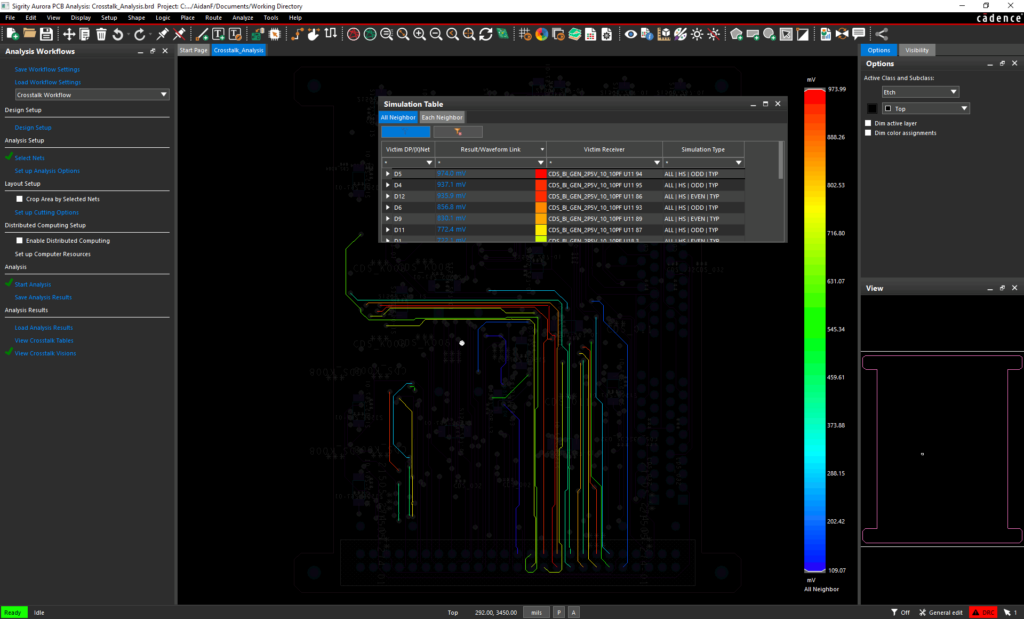
Sigrity Aurora includes easy-to-use workflows that step you through the required procedure to analyze signal and power integrity in your PCB designs. The Crosstalk Workflow in Sigrity Aurora is most commonly used to identify crosstalk in the PCB design, providing a step-by-step procedure to perform layout-based crosstalk analysis directly within the PCB layout canvas. The crosstalk workflow can be used by PCB designers throughout the PCB layout process to identify and correct issue when change is easiest, reducing time spent on prototyping, troubleshooting, and redesigning the PCB. Sigrity Aurora streamlines the product development process and allows you to efficiently analyze crosstalk with:
- A unified environment for PCB design and signal integrity analysis
- Easy-to-use workflows
- Minimal setup and modeling
- Visual overlays directly on the PCB canvas with color-coded results
- Detailed, tabular results to easily pinpoint impedance issues
Learn more about crosstalk and how to resolve them using Sigrity Aurora with our free course: Introduction to In-Design SI/PI analysis with Sigrity Aurora.