 In the current landscape of electronics design, it’s become common for a majority of products to include elements that qualify as “high-speed” in their design. Doing so introduces signal integrity problems; such as electromagnetic interference (EMI) between traces and electromagnetic compatibility (EMC) issues between nearby boards and systems that must be maximally mitigated. This requires PCB designers to familiarize themselves with the challenges high-speed board design present and develop a strategy for successfully addressing these threats to reliable performance. The best solution is to incorporate and follow effective high-speed signal routing guidelines; such as using trace bends and daisy chains to minimize reflections. To aid you, we have assembled a comprehensive list of prevalent PCB design recommendations tailored to optimize the routing of high-speed signals for your PCB design.
Important High-Speed Signal Routing Guidelines
For high-speed board design, it is critically important to follow routing guidelines, as listed below.| HIGH-SPEED SIGNAL ROUTING GUIDELINES | |
| What to do | Why it’s important |
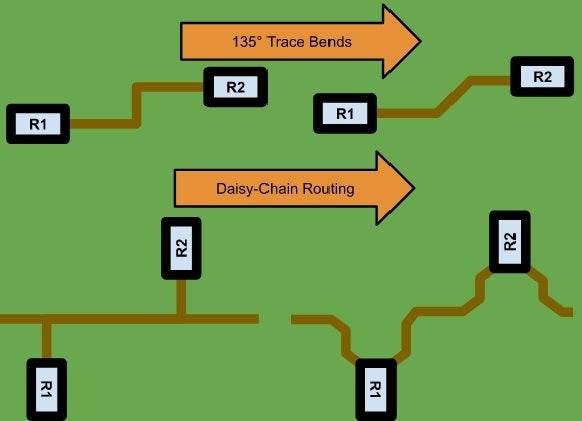
| Opt for 135° Trace Bends | Opt for 135° bends when routing high-speed signals to minimize signal reflection and impedance discontinuities , ensuring smoother signal transitions over traditional 90° bends. |
| Use Serpentine Traces | Use serpentine traces to achieve specific lengths, maintaining a minimum distance of four times the trace width between adjacent parts of the same trace and bend segments at least 1.5 times the trace width. |
| Implement Daisy Chain Routing | Implement daisy chain routing instead of long stubs to preserve signal integrity and meet Electromagnetic Compatibility (EMC) standards ; especially useful when using pull-up or pull-down resistors on high-speed signals to prevent them from acting as antennas or causing signal reflections. |
| Manage the Return Path | Effective management of the return path is crucial for determining a circuit’s overall loop inductance and impedance. This involves setting constraints on the deviation between a signal trace and its reference plane to maintain signal integrity in high-speed PCB designs. |
| Use Short and Direct Routing Paths | Aim for routing paths that are as short and direct as possible, accommodating for specific topologies and required measured lengths that might necessitate deviation. |
| Follow Trace Spacing Standards | Be vigilant of spacing requirements for parallel routing of high-speed transmission lines; such as differential pairs , and follow creepage and clearance standards to prevent crosstalk and ensure signal integrity. |
| Consider Wider Traces for Analog Signals | Opt for wider traces when routing analog signals to enhance performance and reliability. |
As the list above indicates, a good understanding of routing topologies is an asset for effective high-speed signal routing. It is also important to be familiar with common signal integrity issues when designing high-speed PCBs.
Common High-Speed Routing Signal Integrity Issues
Below, we’ve summarized four types of signal integrity issues that may arise if not taken care of during high-speed routing.
- Crosstalk: Influenced by trace spacing and geometry, highlighting the need for careful layout to minimize electromagnetic interference between adjacent traces.
- Reflections: Arise from mismatches in impedance and insufficient termination, emphasizing the importance of matched impedance and correct termination strategies.
- EMI Susceptibility: Tied to loop inductance within trace layouts, suggesting the minimization of loop areas and careful routing to reduce susceptibility to electromagnetic interference.
- Transient Ringing: Different from reflections, though they appear similar, it’s related to loop inductance and board parasitics, indicating a focus on minimizing inductance and managing parasitic elements.
These common problems can be minimized, if not entirely eliminated, by applying the strategies discussed below.
Strategies to Address Signal Integrity Issues
| STRATEGIES FOR ADDRESSING SIGNAL INTEGRITY ISSUES | |
| Strategy | Description |
| Crosstalk Mitigation | Enlarge the distance between traces outside of bottleneck areas to reduce crosstalk, adhering to minimum spacing based on trace length and proximity. |
| Trace and Via Placement and Geometry | Avoid abrupt changes in trace direction and ensure vias do not disrupt impedance continuity and matching. Careful planning of trace geometry and via placement can mitigate reflections and signal loss. |
| Clock Distribution | Minimize path differences to reduce skew and ensure clock signals are properly terminated to avoid reflections. This includes careful layout planning to avoid unnecessary bends and maintaining uniform trace lengths where possible. |
| Optimizing Trace Clearance and Creepage Distances | Control the level of capacitive and inductive coupling with proper trace spacing and width, using electromagnetic solvers to calculate the correct impedance profile for adjustments. |
| PCB Fiber Weave Mitigation | Mitigate signal skew and distortion from fiber weave effects in high-speed applications by routing signals diagonally or using materials with a tighter weave, ensuring more consistent electrical properties across the PCB. |
| High-Speed Signal Reference Plane Continuation | Ensure a continuous reference plane for a consistent return path for signals, reducing loop inductance and mitigating EMI. When signals transition between layers, maintain closely coupled adjacent planes to maintain path continuity. |
Embracing the strategies above will help you improve your board’s signal integrity, provided you prioritize routing guideline implementation for impedance control, differential routing, ground planes, clocks, basic component routing, and other sources of EMI and EMC.
Routing Guidelines for Impedance Control and Differential Routing
When it comes to high-speed designs, a new category of regulations becomes essential, encompassing aspects such as differential pairs, signal paths, routing strategies, ensuring trace lengths are measured and matched, as well as adjustments for trace tuning. These guidelines, although general for routing high speed signals, can be tailored for individual projects, or if incorporated into constraint rules, used across high speed PCBA designs.
- Impedance Control is crucial for preventing signal reflections on electrically long lines due to impedance mismatches. Defining the tolerance for impedance as a design rule helps ensure signal integrity by minimizing back-and-forth reflections.
- High-Speed Signal Trace Lengths and Matching: Precise length matching is crucial for maintaining the phase and timing between differential pairs, reducing bit error rates. Advanced design tools can automate length matching, helping to optimize signal integrity across complex layouts.
- Differential Signal Spacing and Rules reduces crosstalk and electromagnetic coupling between pairs, enhancing signal clarity. Following empirical rules or simulation results can guide optimal spacing for specific signal frequencies and board materials.
- Additional clearance values for sensitive signals, such as clock lines and differential pairs from other routings, typically three times the standard trace width, to minimize interference.
Routing Guidelines for Ground Planes, Vias, and More
During PCB routing design, critical signal lines or specific areas surround the traces with a ground plane to reduce interference, especially for sensitive signals like clock and high-speed analog signals. By adding a protective ground wire around these signal lines, the design minimizes loop formation and system interference.
| TECHNIQUES AND STRATEGIES FOR ROUTING VIAS AND GROUND | |
| Technique/Strategy | Description |
| Route High-Speed Signals Over a Solid Ground Plane | Ensure a solid ground plane underlies the signal traces, covering the entire PCB layer beneath high-speed components. |
| Ensure Continuous Power and Ground Planes | Design continuous ground planes to minimize loop areas and reduce the potential for EMI, avoiding splits or gaps that could interrupt return paths and lead to increased radiation. |
| Avoid Hot Spots with Strategic Via Placement | Implement a grid layout for vias to avoid voids in power and ground planes, spacing vias at least 15 mils apart to minimize hot spots caused by increased current density. |
| Avoid Branches or Stubs | For high-frequency signals on the surface layer, place signal wires between power and ground layers to significantly reduce electromagnetic radiation through absorption. |
| Via Discontinuity Mitigation and Back-Drill Stubs | Back-drilling to remove unnecessary via stubs can reduce reflections and signal loss at high frequencies by mitigating resonant structures. |
| Surface-Mount Device Pad Discontinuity Mitigation | Minimize the impact on signal paths due to pad discontinuities by strategically placing and orienting components and using techniques such as non-conductive via fill to maintain signal integrity. |
| Avoid Routing Over Ground Plane Breaks | Prevent compromising the signal’s clear return path and avoid introducing signal integrity issues by not routing over breaks in the ground plane. |
| Ensure Clear Return Path for High-Speed Signals | Maintain a clear return path on the adjacent ground plane for high-speed signals to support signal integrity. |
| Limit Layer Changes for High-Speed Transmission Lines | Keep layer changes to a minimum for high-speed transmission lines, using a ground via for signal return path transition alongside the signal via, if necessary. |
| Minimize Via Usage | Decrease inductance and improve electrical performance by minimizing via usage, opting for blind, buried, or microvias when necessary. |
Following the best practices above will aid you in optimizing the performance of your high-speed PCBA. However, implementing these guidelines can be a challenge, depending on the EDA tool you use. In many cases, the best option is to utilize product design and development software. Doing so will not only help you ensure the techniques employed for routing high-speed signals are contributing to design efforts to maximize signal integrity and minimize EMI and EMC issues, but also improve your PCBA development efficiency.