Instantaneous and stable power delivery for ICs is necessary to sustain proper circuit operation in today’s high-speed electronics. Decoupling capacitors can be used to provide the necessary power to IC devices; however, it is a delicate balance to achieve adequate power delivery without over-designing. To ensure effective power delivery for your PCB designs, you can obtain insights into decoupling capacitor performance by evaluating the inductive loop.
What is Loop Inductance?
Loop inductance or power inductance refers to the inductance associated with the current loop formed by a signal trace and its return path which includes:
- Stackup
- Routing
- Vias
- Capacitors
In other words, loop inductance is the opposition to change in current flow from the decoupling capacitor to the IC device or the impedance or prevention the PCB has on the capacitor to deliver energy to the IC.
When to Measure Loop Inductance
Loop inductance measurements can be used to help determine if/where power delivery problems would occur as well as provide insights and opportunities to adjust the PDN design. Loop inductance can be used to analyze the responsiveness of the Power Delivery Network (PDN) through:
- Quickly extracting the loop inductance of each capacitor observed from the given devices on a power rail to evaluate effectiveness of capacitor locations
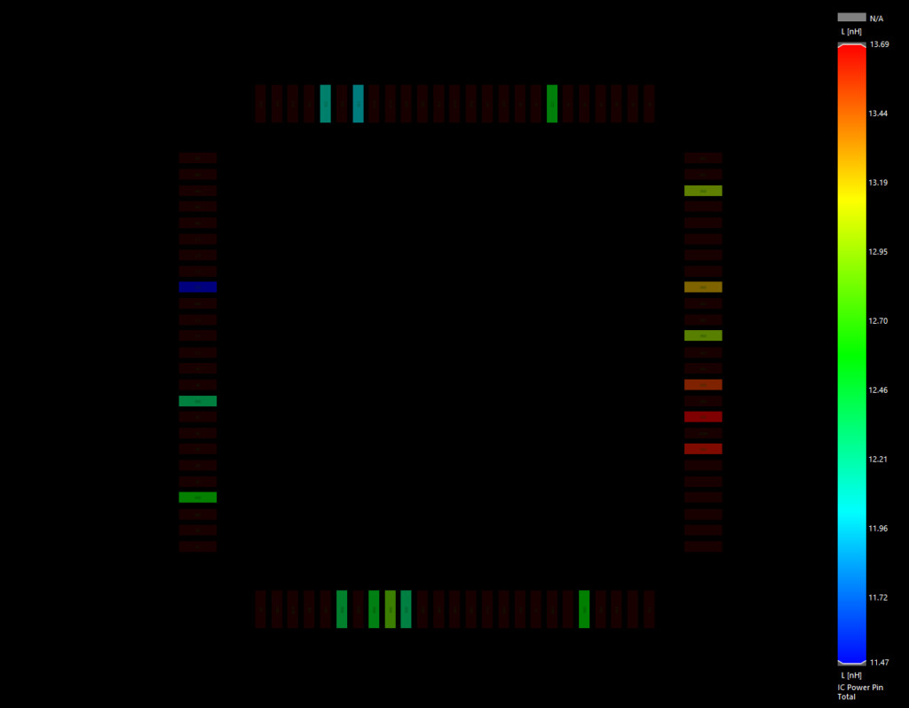
- Quickly calculating the loop inductance of each power pin for IC devices to:
- Identify weak pins
- Meet the different per-pin PDN impedance requirements due to different current of various pins of device
How to Measure Loop Inductance
Inductance is an accumulation, not a physical entity and is very difficult to determine with manual calculations. Software can aid in realistically predicting pin-to-pin inductance by incorporating:
- PCB layout
- Stackup
- Capacitor parasitics
- Capacitor performance
This prediction can be used to control inductance and drive decisions that produce a more responsive power delivery network.
Acceptable Loop Inductance Measurements
The desired power inductance or loop inductance results will vary from circuit to circuit. Typically, loop inductance measurement should be as low as possible to maximize power delivery. The higher impedance of higher-inductance traces can reduce the effectiveness of decoupling capacitors, especially if the circuit is designed to handle potentially noisy signals, such as RF amplifiers or audio processors.
Additionally, for decoupling capacitors on the same chip, loop inductance should be relatively even across the pins.
Common Causes of Insufficient Power Delivery
Insufficient power delivery from high loop inductance can arise from various factors throughout the PCB layout. The table below will help to identify the causes of high loop inductance, why the PCB feature effects power quality, and a solution to help PCB designers identify and optimize power delivery.
| Cause | Problem | Solution |
|---|---|---|
| Poor Decoupling Capacitor Placement | Placing decoupling capacitors far from IC pins creates a longer loop which increases inductance. | Optimize decoupling capacitors. |
| Poor Stackup Design | Return current may take a longer high-impedance path if there is no solid ground or power plane directly beneath the signal layer. | Optimize the PCB Stackup. |
| Poor Via Design | Switching layers with via transitions can force return currents to divert through vias which increases inductance. | Minimize via usage. |
| Long Trace Lengths | The longer the trace length the higher the resistance and inductance. | Optimize trace routing. |
| Improper Plane Design | Split planes, incorrect copper thickness, and the type of copper can all increase inductance. | Improve power and ground plane design. |
Understanding the Impacts of High Loop Inductance
High loop inductance can affect overall system performance and have several negative effects on power quality including the following common power integrity issues:
- Poor Decoupling Capacitor Performance
High loop inductance between decoupling capacitors and IC power pins reduces their effectiveness at suppressing high-frequency noise and delivering instantaneous power as required.
- Intermittent Failures
Issues within the power delivery network are difficult to identify and troubleshoot, are often inconsistent, and produce failures intermittently.
- Unreliable Data Transmission
Even an IC with ample current supply can experience a power shortage if the energy needed to transmit the data bitstream isn’t available. This can result in unreliable data transmission.
- Signal Integrity Problems
In fast signal transitions, high loop inductance can result in common signal integrity issues such as ringing, reflections, and overshoot/undershoot. This can lead to data errors and incorrect operation.
- Increased Timing Errors
Inductance resists changes in current which can cause slower rise and fall times in digital signals, affecting timing and signal synchronization.
- Increased Ground Bounce
High loop inductance, specifically in the return path, can increase ground bounce. Nearby traces my experience additional crosstalk which can degrade overall system reliability.
To prevent these issues, PCB designers must try to create a stable and reliable power delivery network through loop inductance optimization strategies.
Optimization Strategies for Loop Inductance
High loop inductance must be addressed to improve power quality in your designs, ideally during the PCB design process when change is easiest to implement. To correct high loop inductance, the following strategies can be utilized:
1. Optimize Trace Routing
Minimize the length and loop area of signal traces by routing them close to their return paths. Optimize fanouts by adjusting the direction of the vias and the distance between vias and the capacitor to improve inductance.
- Keep the Loop Short
- Optimize Fanouts
2. Optimize Decoupling Capacitors
Every capacitor has an effect on PDN responsiveness. Place decoupling capacitors close to power pins of components to filter noise and stabilize the power supply. Additionally, place all capacitors on the top layer of the PCB. This will minimize the distance to the plane, keep the loop short, and improve performance. Ensure proper power delivery can be achieved and adjust the size of the capacitor as required.
- Place Decoupling Capacitors Close to ICs
- Place Decoupling Capacitors on the Top Layer
- Optimize Capacitor Size
3. Improve Power and Ground Planes
Ensuring continuous and solid ground and power planes will help provide low inductance return paths. Verify that the type of copper used is best for the design and increase the amount of copper to improve power delivery.
- Use Solid Ground and Power Planes
- Increase Copper
4. Optimize the Stackup
Keep power and ground planes adjacent and close to the top layer (where the decoupling capacitors should be placed) to minimize the distance to the plane.
- Keep Power and Ground Planes Adjacent
- Place Power and Ground Near Top Layer
5. Minimize Via Usage
Analyze the via design and via size to determine if it is acceptable for the required power delivery. To minimize via inductance, reduce the use of vias and ensure that when used, they are designed to have low inductance.
- Optimize Via Design and Size
- Reduce Number of Vias Used
Implementing these optimization strategies throughout the PCB design process can result in many benefits and allow you to set the design up for success. But identifying power delivery issues in the design may be difficult and time-consuming which leads to the question- how do you know when and where to deploy these optimization strategies?
Incorporating Simulation
To ensure stable and instantaneous power delivery for ICs in your PCB designs, simulation can be deployed to quickly assess loop inductance and pinpoint areas of high inductance. Simulation tools typically calculate and validate loop inductance based on the PCB layout and can be used to analyze power integrity and identify loop inductance issues created by:
- Poor decoupling capacitor placement
- Incorrect decoupling capacitor size
- Excess via usage
- Incorrect trace length or width
Once these issues are identified, optimization strategies can be incorporated into the PCB design to improve power integrity and the power delivery network.
Why Should You Analyze Loop Inductance?
Analyzing loop inductance and implementing optimization strategies will improve overall PDN performance by guaranteeing ICs receive the required power instantaneously. Performing power inductance or loop inductance analysis can benefit your PBC design process to:
- Optimize Decoupling Capacitors
By analyzing loop inductance, you can guarantee the effectiveness of decoupling capacitors in your design and optimize performance by adjusting the location and size.
- Identifying Weak Power Pins
Analyze IC power pins, identify weak pins, and meet the different per-pin PDN impedance requirements due to differences in current or various pins of devices.
- Optimize the PCB Layout
Analyzing loop inductance helps identify critical areas of the PCB where inductance needs to be minimized. Loop inductance can be reduced by modifying aspects of the design including:
- Trace routing
- Via placement
- Ground plane design
- Increase Responsiveness
Analyzing the loop inductance on the PCB will ensure decoupling capacitors can provide instantaneous power when required. Analyze the stackup, layout, and capacitor parasitics to simulate realistic loop inductance and guarantee a responsive and effective power delivery network.
- Reduce Troubleshooting Time
Incorrect size and placement of decoupling capacitors can result in intermittent power shortages, which are difficult to pinpoint and troubleshoot. Analyzing loop inductance during the PCB layout can help identify issues quickly and minimize the time spent troubleshooting in the lab.
Performing loop inductance analysis at any stage of the design is going to yield benefits but having this as the last step in your design process can result in late-stage design changes, additional rework, and more design hours if any issues are found. Analyzing power inductance throughout the PCB layout will allow you optimize your PDN design and ensure adequate and reliable power delivery- this is where Sigrity Aurora can help.
Analyzing Loop Inductance with Sigrity
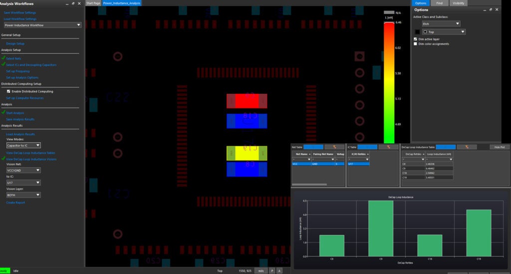
Sigrity Aurora includes easy-to-use workflows that step you through the required procedure to analyze signal and power integrity in your PCB designs. The Power Inductance Workflow in Sigrity Aurora is most commonly used to analyze loop inductance, providing a step-by-step procedure to perform layout-based power inductance analysis directly within the PCB layout canvas. The Power Inductance workflow can be used by PCB designers throughout the PCB layout process to identify and correct issue when change is easiest, reducing time spent on prototyping, troubleshooting, and redesigning the PCB. Sigrity Aurora streamlines the product development process and allows you to efficiently analyze loop inductance with:
- A unified environment for PCB design and power integrity analysis
- Easy-to-use workflows
- Minimal setup and modeling
- Visual overlays directly on the PCB canvas with color-coded results
- Detailed, tabular results to easily pinpoint high loop inductance
Learn more about loop inductance and how to resolve common power integrity issues using Sigrity Aurora with our free course: Introduction to In-Design SI/PI analysis with Sigrity Aurora.