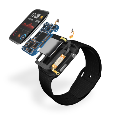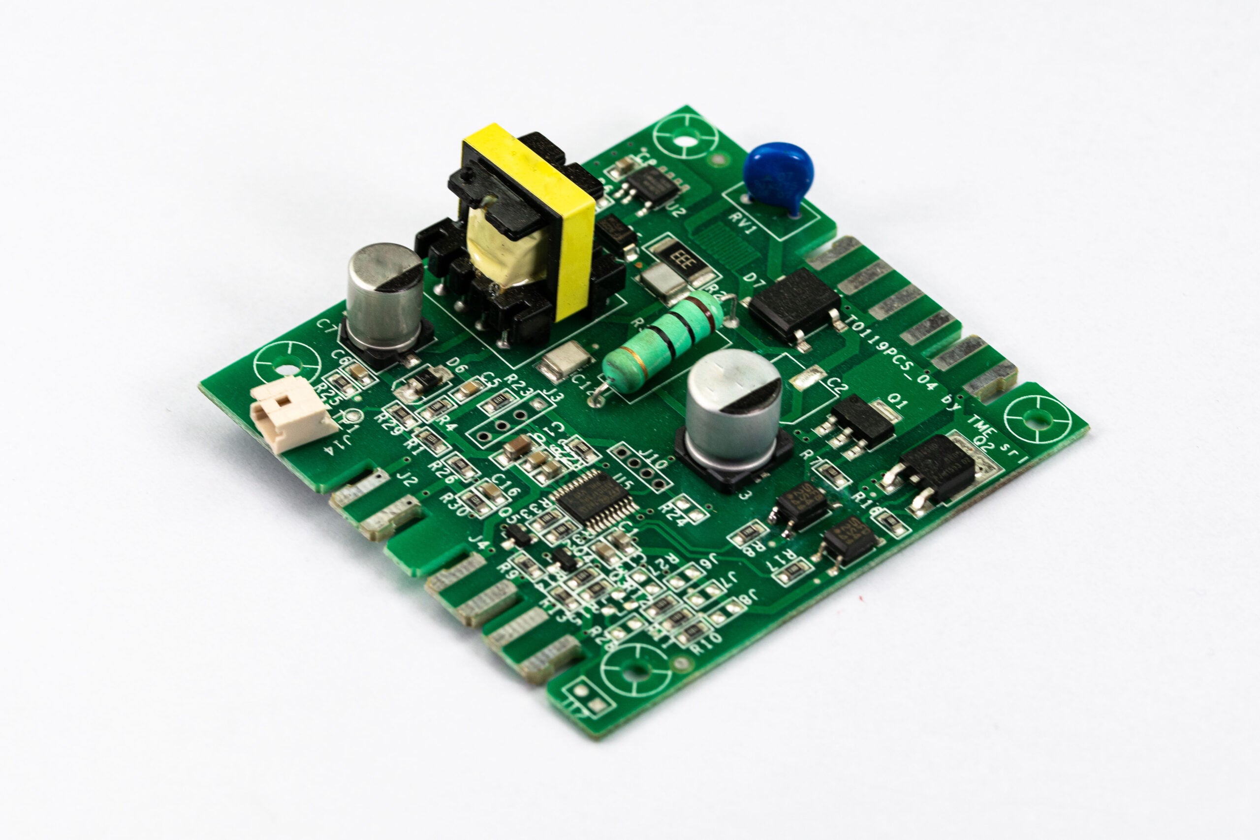
Electronic power supplies are everywhere, even in your favorite coffee grinder. All PCBs utilize electrical energy, and virtually all circuit boards include some type of power distribution network (PDN) to ensure that all elements get the energy they need when they need it. Successful power supply design necessitates a good understanding of power integrity basics and following the best power supply layout guidelines.
Power Supply Layout Guidelines for PCB Design
The major classifications of power supplies are linear and switch-mode. Linear power supplies have better noise immunity, but are less efficient. SMPSs are very efficient, yet the use of high-speed switching can lead to greater electromagnetic interference (EMI) and electromagnetic compatibility (EMC) issues. Many layout guidelines apply to either type; however, there are distinct considerations that should be prioritized for each, as listed below.
| Major Power Supply Layout Guideline Considerations | ||
| Considerations | Linear Power Supply | Switch-Mode Power Supply (SMPS) |
| Component Placement | Place the voltage regulator for maximum airflow, typically near the board edge. | Place components to minimize trace lengths. |
| Grounding Technique(s) | Ground planes should be solid to avoid introducing noise and thermal hot spots. | Use separate grounds for AC input and DC output circuits. |
| Thermal Simulations | Use heat sinks and thermal vias liberally. | Use heat sinks, thermal vias, and thermal reliefs to dissipate heat from hot spots. |
| Safety and Compliance | Follow IPC-2221 and IPC-2152 guidelines for safe creepage and clearance and current carrying capacities, respectively. | EMI and EMC are the primary concerns for SMPSs. Important standards are 47 CFR 47 Part 15 A & B, as well as IEC 61000 Series. |
As shown above, there are four primary areas of consideration for power supply layout design. Following the guidelines for each is critical for your linear or SMPS design.
Component Placement for Optimal Performance
Strategic component placement is important irrespective of your power supply design type. Inadequate spacing and clearance can adversely impact thermal management and electromagnetic compatibility. Guidelines for optimal component placement include:
- Avoid clustering high-power components
- Isolate noise-sensitive circuits
- Follow creepage and clearance distance standards
- Apply a sound decoupling strategy with capacitors close to pins
It is also important to pay special attention to the placement of high-current components. Some examples are listed below.
| High-Current Component Placement Guidelines | |||
| Component Category | Placement Priority | Thermal Consideration | EMI Impact |
| Power MOSFETs | Heat sink access | Primary heat source | High switching noise |
| Power Inductors | Airflow path | Moderate heating | Magnetic field coupling |
| Rectifier Diodes | Thermal relief | High power dissipation | Conducted noise |
| Filter Capacitors | Load proximity | Minimal heating | Ripple current handling |
| Current Sense Resistors | Signal path | Moderate heating | Precision requirement |
Grounding Techniques for Power Supply Layout Design
Proper grounding forms the foundation of successful power supply design, yet many engineers underestimate its complexity. Effective grounding strategies eliminate ground loops, reduce EMI, and ensure stable operation across varying load conditions. Good tips for power supply layout include:
- Separate analog and digital ground planes, if possible.
- Pair power and ground planes in your stackup
- Employ single-point and multi-point grounding for frequencies between 1 and 10 MHz and above 10 MHz, respectively
The table below provides additional guidance on designing your grounding system.
Ground System Design Matrix
| Grounding Options for Power Supply Layout Design | ||||
| Ground Type | Frequency Range | Implementation | Noise Immunity | Complexity |
| Single-Point | DC - 1MHz | Star configuration | Excellent | Low |
| Multi-Point | > 1MHz | Plane-based | Good | Medium |
| Hybrid | DC - 100MHz | Combined approach | Very Good | High |
| Segmented | Mixed-signal | Separated planes | Excellent | High |
Thermal Simulation and Analysis
When designing power supply layouts, it is essential to perform thermal simulation and analysis. Thermal simulation identifies potential hot spots and validates thermal management strategies before prototype fabrication. Depending on your PCB design software, thermal analysis capabilities may be integrated. If not, it may be necessary to add a support simulation software program.
Following effective thermal design guidelines is important to help you optimize your layout for safety and operation. Accurately modeling your board is essential to obtain usable results on which you can base a solution strategy. Tips for performing thermal simulation include:
- Include material properties, component dissipation rates, and environmental conditions
- Define acceptable temperature ranges
- Prioritize high-power components and traces
- Iteratively revise the design by repositioning components and adding thermal vias and reliefs until all hot spots and potential thermal issues are resolved
Safety and Compliance Considerations
Power supply designs must meet safety standards and regulatory requirements while maintaining optimal performance. Understanding key compliance requirements during the design phase prevents costly redesigns and certification delays. Important standards for power supply layout design are:
- IPC-2221 provides specific spacing requirements that ensure safe operation under various environmental conditions
- IPC-2152 standards for current-carrying capacity
- CFR 47 Part 15 A & B for managing EMC
Applying the Best Power Supply Layout Guidelines to Your PCB
Optimizing your board design and instituting the best power supply layout guidelines begins with understanding the type of power supply you are working with and how that will affect the power supply behavior and the layout. The table below lists a linear topology power supply, followed by many different types of SMPS topologies, including Buck, Boost, and many others.
| Power Supply Topology Comparison Matrix | |||||
| Topology | Efficiency | Heat Generation | Layout Complexity | Noise Level | Best Applications |
| Linear | 30-60% | High | Low | Very Low | Low-noise analog circuits, audio |
| Buck Converter | 85-95% | Low | Medium | Medium | Step-down DC-DC conversion |
| Boost Converter | 85-92% | Low | Medium | Medium | Step-up DC-DC conversion |
| Buck-Boost | 80-90% | Medium | High | Medium-High | Voltage regulation, battery systems |
| Flyback | 70-85% | Medium | High | High | Isolated supplies, multiple outputs |
| Forward Converter | 80-90% | Medium | High | Medium | Higher power isolated supplies |
| Full-Bridge | 85-92% | Low | Very High | Medium | High-power applications |
| Bridge Rectifier | 95-98% | Low | Low | Low | AC-DC conversion front-end |
To learn how to ensure your boards deliver long-term, reliable operation, see our Ebook on Optimizing Power Supply Design.