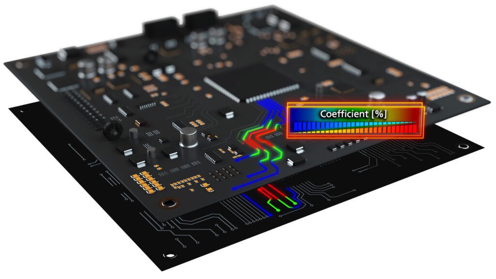
In PCB design, grounding isn’t just a box to check — it’s the foundation that supports your entire circuit. Without solid grounding practices, your board is vulnerable to instability, noise, electromagnetic interference (EMI), or even safety hazards.
Understanding where grounding physically occurs in a PCB layout helps you place components, create planes, and route traces more effectively. Applying smart PCB layout grounding techniques is key for designing complex circuit boards. This article walks you through everything you need to know about proper grounding, types of grounds, and PCB layout grounding techniques.
Important Locations for PCB Grounding
| PCB GROUNDING LOCATIONS AND FUNCTIONS | |
| Location | Function |
| Power entry | Interface for chassis and earth ground |
| Return paths | Ensure minimal impedance and loop area |
| Mixed-signal boundaries | Separate analog and digital return currents |
| I/O interfaces | Manage ESD and EMI at connector shields |
As shown above, several board locations require special considerations when laying out your PCB grounding techniques.
Core PCB Grounding Techniques
Now, let’s get tactical. For circuit boards to operate effectively, core PCB grounding techniques must be employed. Chief among these are dedicated ground planes and the use of short return paths and reference planes.
Dedicated Ground Planes
Dedicated ground planes are continuous, unbroken ground layers within the PCB stackup, which yield the following benefits for signal propagation.
- Reduce impedance dramatically
- Provide a low-noise return path for high-speed signals
- Act as a shield against EMI
| Pro Tip: In a 4-layer board, use the second layer as a solid ground plane under the top signal layer. This creates a microstrip configuration for controlled impedance. |
When implementing dedicated ground planes, the following guidelines should be followed:
Guidelines for Dedicated PCB Ground Planes
|
Short Return Paths and Reference Planes
Another important consideration, which is often overlooked, is the importance of grounding for safety on PCBs. Noting that current takes the path of least impedance — not the least distance–is a good way to remember to route traces over solid ground planes and use ground vias to maintain tight return loops.
| Pro Tip: Crossing a split plane without planning for return paths guarantees EMI headaches. |
Common PCB Ground Types
In order to effectively apply PCB grounding techniques, it is pertinent to know the various PCB ground types. These are explained in the table below:
| PCB GROUND TYPES | |
| Ground Type | Purpose and Notes |
| Power Ground | DC return for power signals. Needs separation from signal ground. |
| Signal Ground | Reference for voltage measurements. Must stay clean and stable. |
| Virtual Ground | Special use in op-amps — not tied to a ground plane. |
| Floating Ground | Unreferenced or isolated system ground. Reduces ground loops. |
| Earth Ground | Physical ground for safety. Especially important in high-voltage systems. |
| Chassis Ground | For shielding, ESD protection, and mechanical grounding. |
PCB Layout Grounding Techniques: Application in Layout
Now, let’s get into the practical PCB layout grounding techniques that are based on the cores discussed above. These include using bypass and decoupling capacitors, stitching vias, and via fencing.
Bypass and Decoupling Capacitors
Placing capacitors between a device’s power and ground pins, either to route noise to ground (bypass) or provide energy stability (decoupling), are important grounding techniques in high-power designs. Benefits include:
- Reduce voltage spikes
- Minimize ground bounce and ringing
- Help maintain clean power rails
| Placement Tip: Place capacitors close to the device pins. Use short traces and direct connection to the ground plane. |
Stitching Vias and Via Fencing
Stitching vias, which connect conductors between layers, and via fencing, which provides a barrier between components and circuitry, are also useful PCB ground techniques. When used, follow the guidelines below.
Guidelines for Via Stitching and Fencing
|
| Example: For a 2.4 GHz signal, vias should be spaced every ~6 mm (¼ inch or less). Use simulation to verify stitching effectiveness. |
Special Grounding Considerations for High-Power and HDI Boards
High-current and/or high-density interface (HDI) designs introduce new grounding challenges, such as the need for signal-type isolation. Effective techniques for addressing this issue are galvanic isolation, which separates high-voltage and low-voltage circuits, and split planes, which separates analog and digital circuitry. Follow the guidelines below when employing these techniques:
Guidelines for Galvanic Isolation
|
| Pro Tip: For those especially complicated designs, consider using simulations to ensure proper grounding. |
Guidelines for Split Planes
|
Additional PCB Grounding Techniques
Less common PCB grounding techniques include guard traces, hatched ground fills, and via-in-pad. If used, the following guidelines are helpful to keep in mind:
Guidelines for Additional PCB Grounding Techniques
|
Before placing components or routing traces, it is a good idea to define your grounding strategy and consider which PCB layout grounding techniques to use to implement it. The ability to implement many of these grounding techniques depends on the quality of your PCB design software. With OrCAD X, you are well-equipped with the best EDA tool for implementing core and specialized grounding techniques. For assistance with the right tool and/or support to design the grounding needed for your project, it is advisable to partner with the industry leader in supporting PCB design engineers.
EMA Design Automation is a leading provider of the resources that engineers rely on to accelerate innovation. We provide solutions that include PCB design and analysis packages, custom integration software, engineering expertise, and a comprehensive academy of learning and training materials, which enable you to create more efficiently. For more information on PCB grounding techniques and how we can help you or your team innovate faster, contact us.