Crosstalk is a major source of signal integrity problems on and in PCBs. Often, the root cause is unintentional coupling between nearby conductive elements (most often traces). Generally, designers spend a significant amount of time evaluating intraplanar coupling, with the classic example being two non-differential pair signals routed too close together in parallel for an extended stretch. However, interplanar crosstalk is also possible and can be more insidious due to the difficulty of identifying and quantifying its impact between two signal layers. The influence of PCB cores on crosstalk can disrupt a design and lead to costly retesting and revisions, so avoiding some common pitfalls is in any designer’s best interest.
| The Influence of PCB Cores on Crosstalk by Modality | |||
| Description | Core-Dependent | Solution | |
| Edge coupling | Coupling between the thickness of conductors, i.e., intraplanar coupling | No | Provide ample space according to 3W rule of thumb |
| Broadside coupling | Coupling between the width of conductors, i.e., interplanar coupling | Yes | As above, but consider signal integrity of stackup w.r.t. reference planes |
Examining the Influence of PCB Cores on Crosstalk
The core of a circuit board–which is most often physically located at the geometric mean of the stackup–is fabricated from a laminate, a substrate material with copper foil attached on its top and bottom surface. The copper foil goes through an etching process that leaves the traces and removes all other excess copper. Based on Ampere’s Law, rotating magnetic fields surround current-carrying traces that are proportional in strength to the signal. The intensity of these magnetic fields diminishes rapidly with distance. However, when the field is strong enough or an adjacent conductor is close enough (and parallel to the direction of the aggressor conductor for maximum coupling), it’s possible to induce a current on the victim line. Critically, it’s the speed of the signal that impacts the coupling potential, and high-speed designs are where concerns about crosstalk are most prominent.
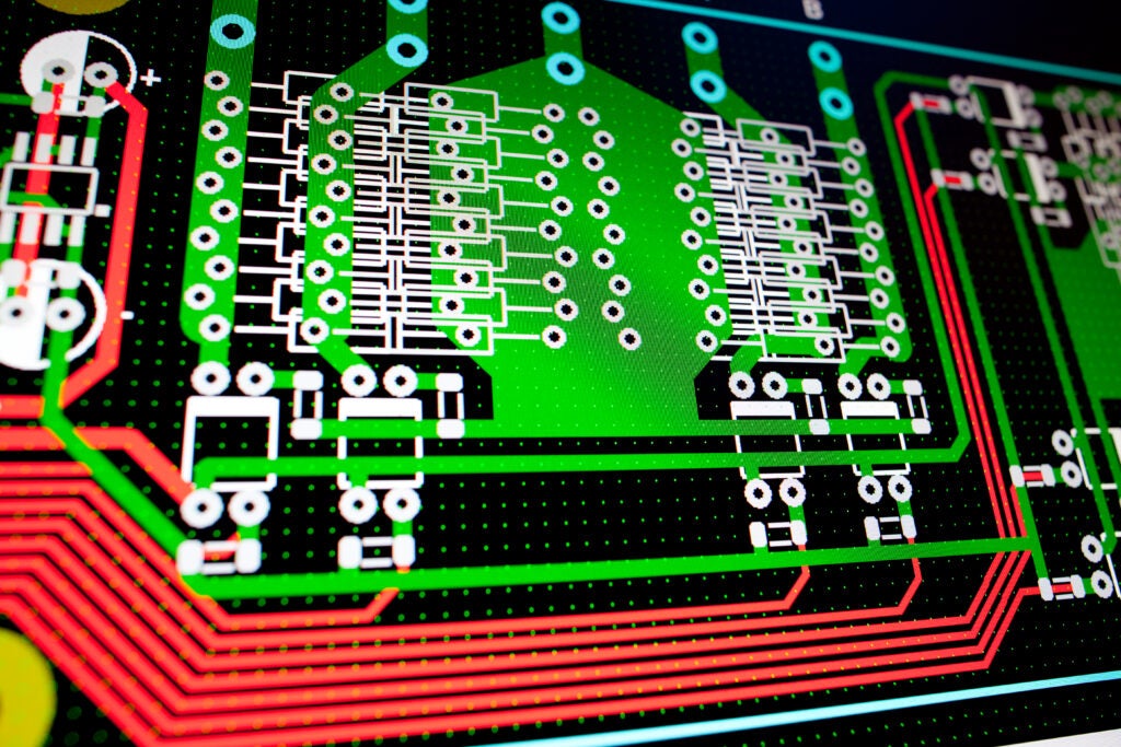
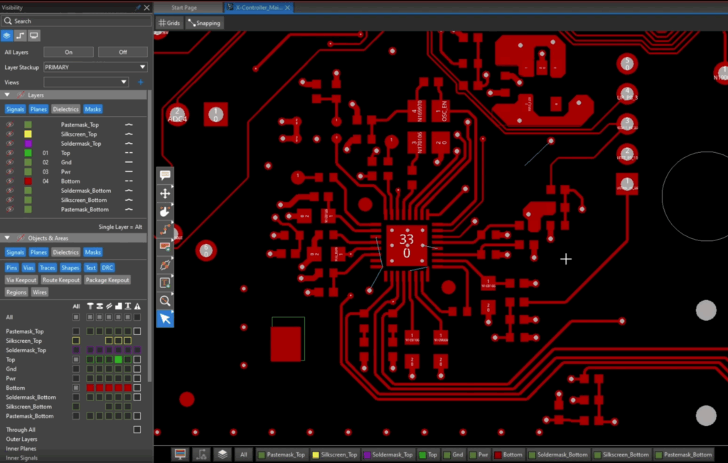
Within most ECAD software, setting up the design rule check (DRC) to limit interplanar crosstalk is trivial: simply set the minimum trace gap globally or on a case-by-case basis. Generally, designers use the 3W rule for trace spacing – if the smallest trace width measures four mils; the smallest gap measured center-to-center would be 12 mils. In this example, the minimum air gap between two conductors would be 8 mils (3 * minimum trace thickness – 2 * (minimum trace thickness/2)). This rule of thumb becomes more inexact when talking about distance through a laminate, but it provides a rough and familiar estimate for designers.
How Designers Minimize Crosstalk
Fortunately, designers have multiple layout approaches to minimize the influence of PCB cores on crosstalk:
- One of the easiest ways to avoid crosstalk when routing traces in parallel on adjacent signal layers is to use a cross hatching method. Begin by identifying a preferred orientation for traces on the first signal layer, typically the top layer. For each subsequent signal layer, alternate a primarily vertical or horizontal orientation. Because coupling depends on the dot product (i.e., the parallel component) between two conductors, completely perpendicular trace pairs have zero crosstalk capability.
- If possible, a thicker core will dissuade the coupling ability between traces on adjacent signal layers. A PCB core with a thickness of at least 3x the minimum trace gap is ideal, but the physical dimensions of the board and the electrical characteristics of the stackup take precedence. If possible, avoid 5 and 8 mil cores, and consider whether a 14 mil core will be thick enough for the minimum trace width.
- Ensure a balanced PCB stackup about the core: the number of layers, the material distribution (i.e., laminate and prepreg), the impedance symmetry, and the signal/ground plane assignment. The last aspect is critical, as power and ground planes provide voltage references for signal traces throughout the design. By ensuring that signal planes have adjacent reference planes throughout the stackup, current return paths remain short and minimize the deleterious effects of electromagnetic interference (EMI).
EMA Supercharges PCB Design
It’s easier to overlook PCB core crosstalk that occurs between planes rather than within a plane, but failure to account for this insidious source of EMI can sink a design during electromagnetic compatibility (EMC) testing. Looking to learn more about how the physical makeup of a board affects performance? EMA Design Automation offers simulation products and training to analyze the dielectric effects of your board and help you improve PCB layout workflow for superior performance.
EMA Design Automation is a leading provider of the resources that engineers rely on to accelerate innovation. We provide solutions that include PCB design and analysis packages, custom integration software, engineering expertise, and a comprehensive academy of learning and training materials, which enable you to create more efficiently. For more information on the influence of PCB cores on crosstalk and how we can help you or your team innovate faster, contact us.


