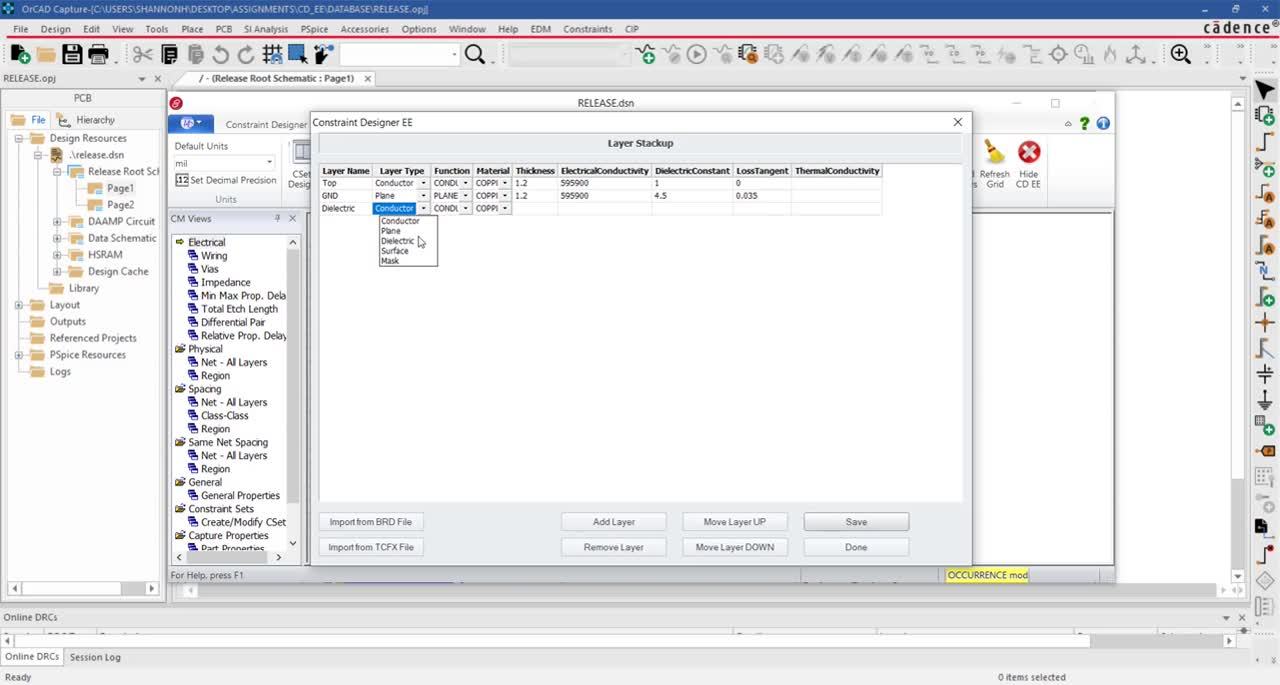
Defining the design specifications at the schematic level, results in less room for interpretation in the PCB layout. However, managing rules for multi-layer boards becomes extremely difficult with spacing, line width, and rules for differential pairs or DDR’s defined on a layer by layer basis. With Constraint Designer EE, accurate rules can be defined and managed by incorporating the layer stack up of the PCB by:
- Creating a layer stack up by adding, removing, and editing layers
- Importing an existing board file
- Creating layer specific constraints for spacing, line width, vias and neck
- Defining layer specific rules for differential pairs and DDRs
- Defining layer sets to ensure nets are only routed on specific layers
By creating detailed, layer-based rules you can accurately communicate your design intent from schematic to PCB with Constraint Designer EE.
