The more engineers working on a project, the likelihood of errors due to miscommunication increases. In the design process, many errors due to ineffective communication can occur between the schematic completion and the PCB design. By defining and embedding the constraints at the schematic level with Constraint Designer EE, you can communicate your design intent from schematic to PCB with these five steps:
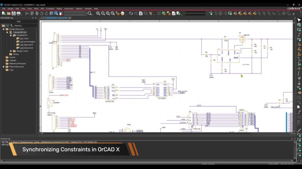
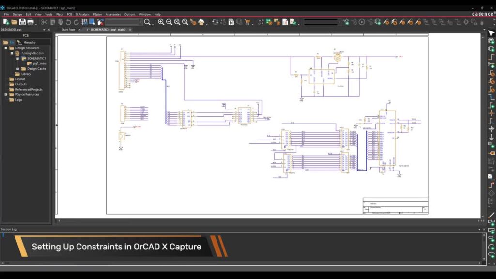
Step 1: Specify the physical and electrical requirements during the schematic.
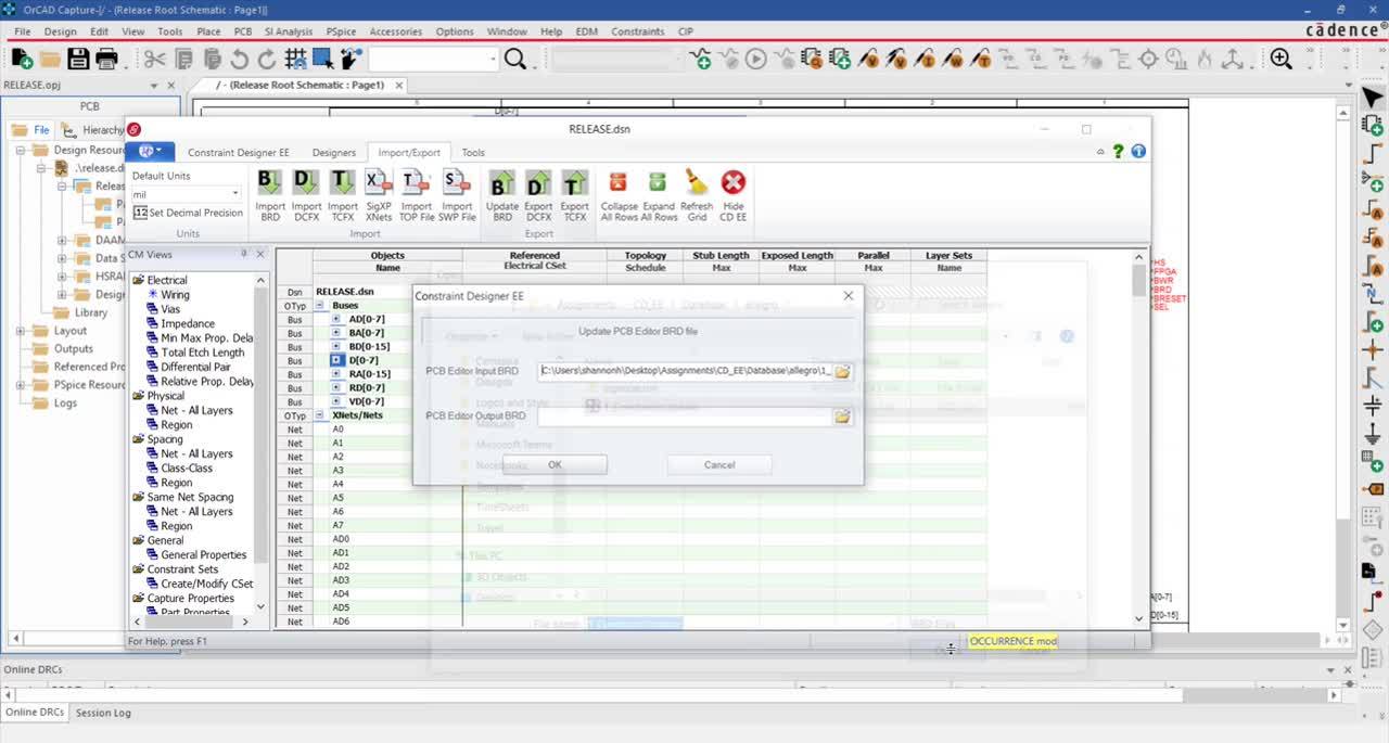
Step 2: Push the embedded constraints directly from Constraint Designer EE to OrCAD PCB Designer.
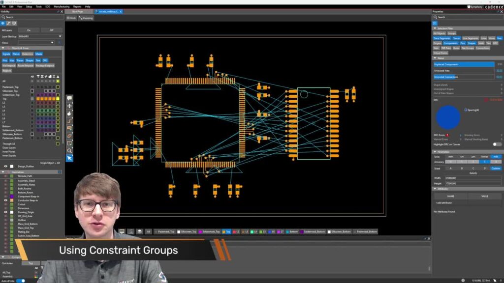
Step 3: Open the constraint manager in OrCAD PCB view the automatically applied rules.
Step 4: Analyze errors by locating DRC markers.
Step 5: Push rule changes from the PCB design into Constraint Designer EE in OrCAD Capture.
Constraint Designer EE makes communication of your design constraints simple with a seamless bidirectional connection between schematic and PCB design.