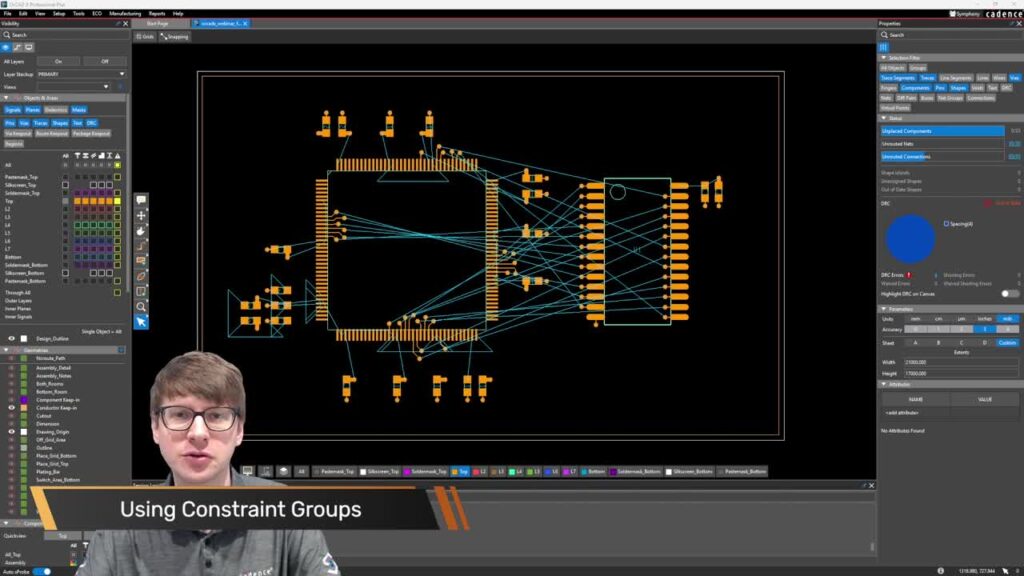
In OrCAD X 25.1, padstacks can be modified directly in the OrCAD X layout environment. With selection of a padstack in the PCB canvas, padstack holes and stackups can be previewed in the properties panel for efficient review. If modifications are required, edits can be made directly within the properties panel such as:
- Layers
- Pad types
- Geometry
- Copper pad properties and features
- Pastemask pad properties and features
- Soldermask pad properties and features
- Finished diameters
For more advanced options, the padstack editor can be launched directly from the properties panel to modify pins throughout the PCB layout.
Learn more about OrCAD X 25.1 here and test out this feature and more with a free trial.