PRODUCT FEATURE

In-Design Analysis

What is In-Design Analysis?

In-design analysis in PCB design refers to the process of performing real-time, automated checks and simulations within the PCB design environment. This approach helps designers identify and address potential issues during the design phase rather than post-design, reducing the need for extensive rework and improving the overall quality and reliability of the PCB.

Benefits

  • Easy to Use Intuitive Simulation Environment
  • Improved Signal Integrity and Power Integrity
  • Minimize Late-Stage Design Changes
  • Efficient Identification of Errors During the Design
  • Unified Environment for Design and Analysis

Try In-Design Analysis with OrCAD X

In-Design Analysis in OrCAD X

In-Design analysis can be performed directly in the PCB canvas to verify electrical performance and improve signal and power integrity in OrCAD X. Visual color-coded overlays and tabular results help engineers pinpoint issues that are typically hard to find in the lab enabling them to identify and correct problems early in the design process when change is easiest. The easy-to-use and configure simulations make signal and power integrity analysis accessible and understandable for all users without being an SI/PI expert and allow you to analyze:
  • Impedance
  • Coupling
  • Reflections
  • Crosstalk
  • IR Drop
  • Return Path
  • Loop Inductance

Key Features for In-Design Analysis with OrCAD X

OrCAD X contains the functionality you need to perform in-design analysis efficiently.
Unified Design Environment
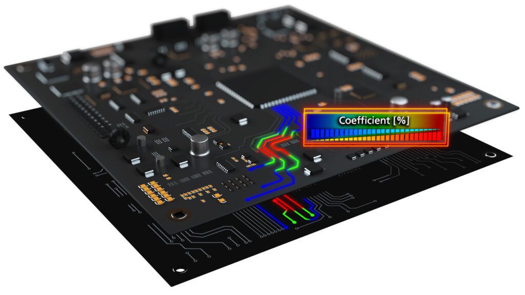
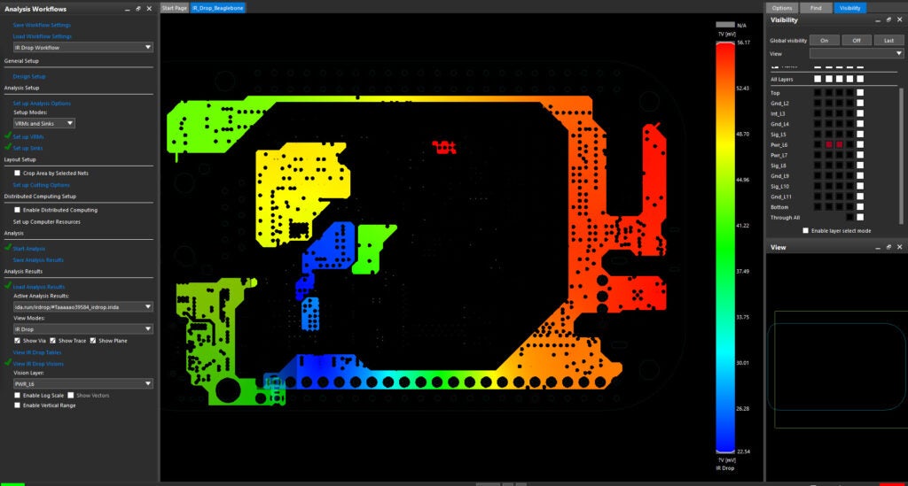
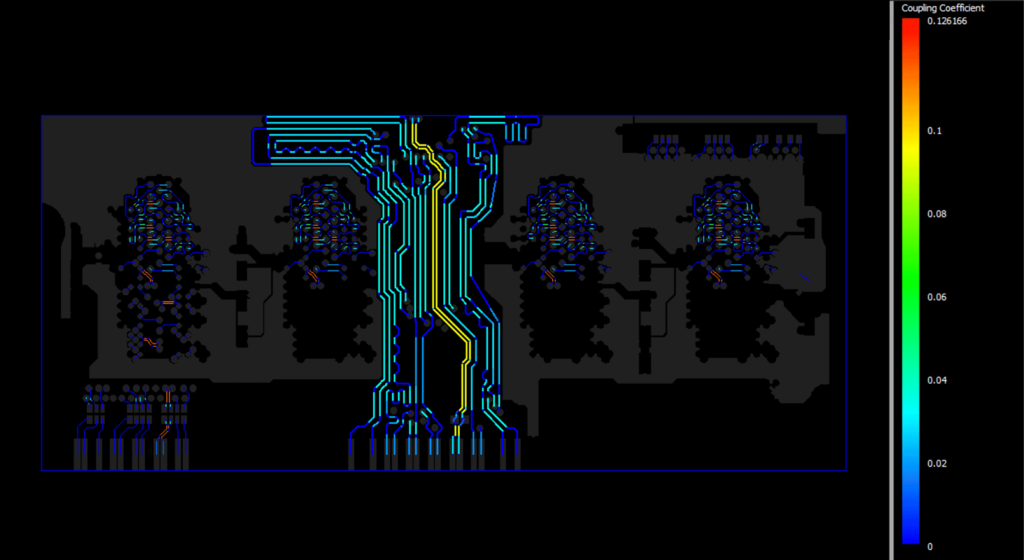
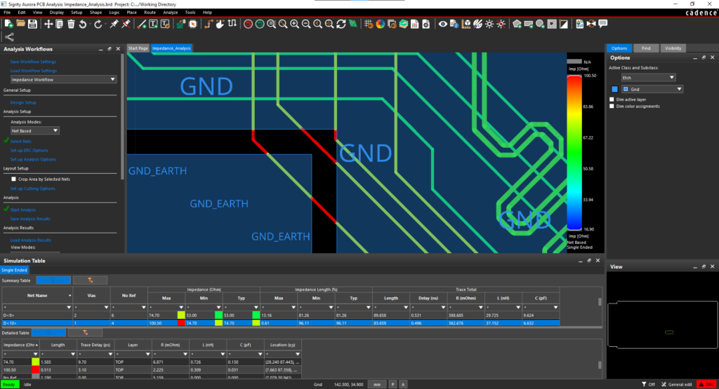
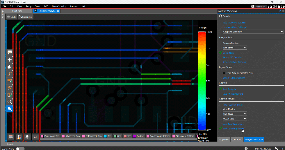
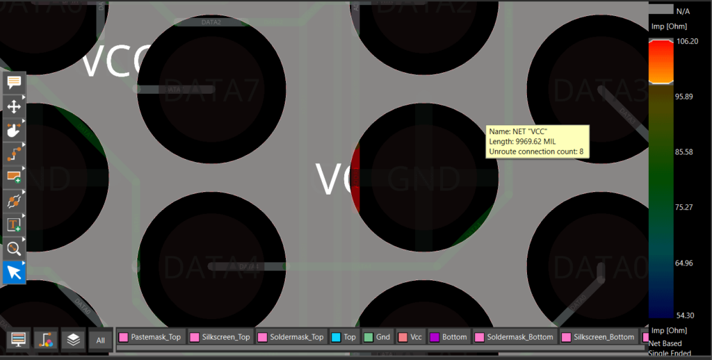
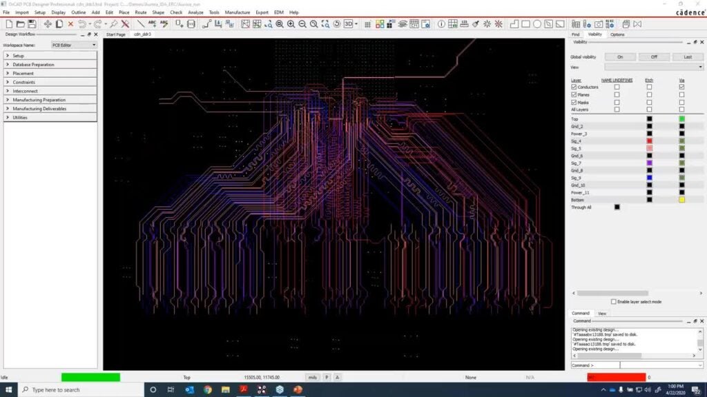
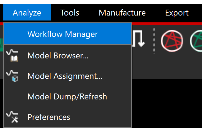
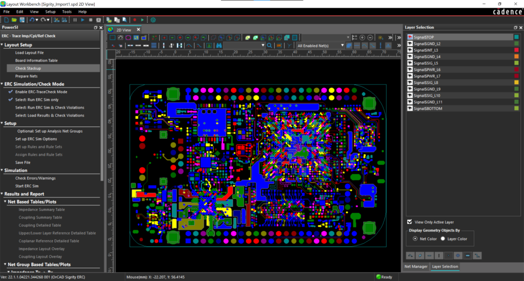
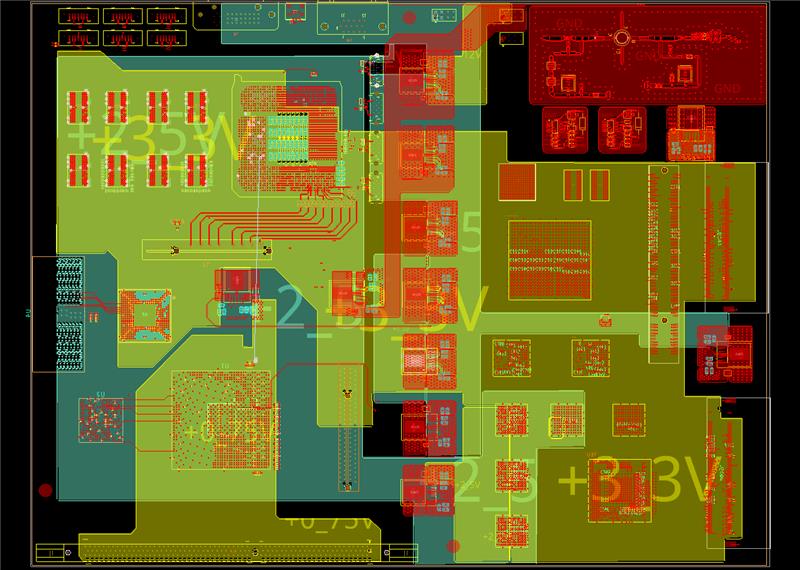
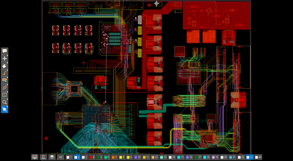
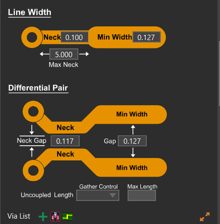
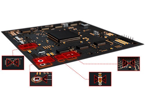
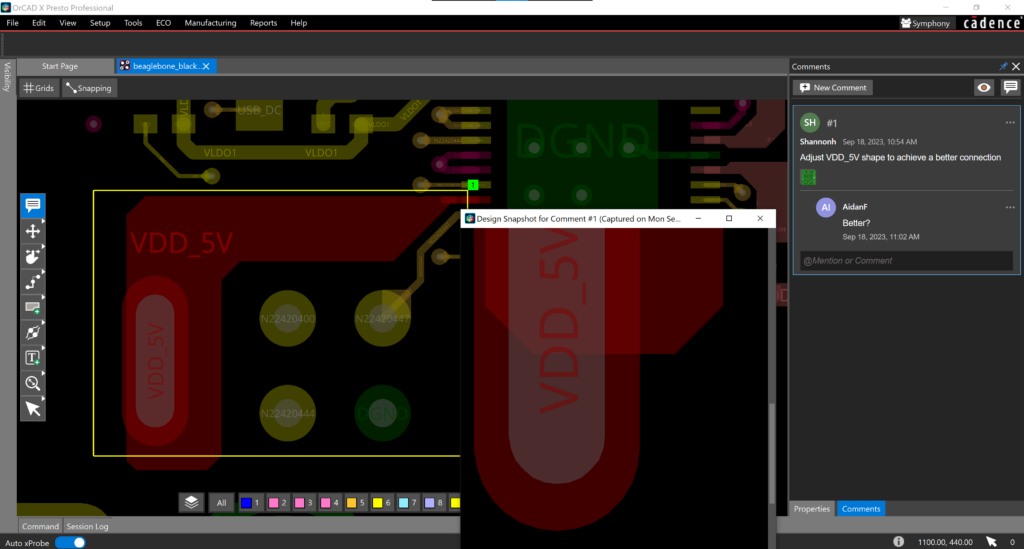
In-design analysis in OrCAD X provides one environment to complete your PCB design and perform common signal integrity and power integrity analysis. The unified environment provides a common interface, minimizing the requirements to learn additional software, and allows you to design, analyze, and modify the PCB without transitioning between tools.
Visual Overlays
In-design analysis results are displayed with visual overlays directly on the PCB allowing you to efficiently pin point signal integrity and power integrity problems. Visual overlays are color-coded with an adjustable scale for quick identification and modification of the PCB design.
Tabular Results
Tabular results provide detailed information on your signal integrity and power integrity analysis. Numerical results are color-coded for efficient identification and problems can be identified on the PCB with cross-probing technology between results and the design canvas.
Sigrity Aurora
Signal Integrity Analysis
Perform in-design analysis to identify common signal integrity issues in your PCB with impedance analysis and coupling analysis in OrCAD X Professional. Expand these capabilities with Sigrity Aurora incorporating easy-to use workflows for crosstalk analysis and reflection analysis.
Sigrity Aurora
Power Integrity Analysis
Perform in-design analysis to identify common power integrity issues in your PCB with IR drop analysis, current density analysis, return path analysis, and power inductance analysis.
Simplified Configuration
In-design analysis in OrCAD X provides a simplified approach to signal integrity and power integrity analysis with the required steps detailed in an easy-to-use workflow, minimal simulation setup, and pre-configured simulation models -making SI and PI analysis accessible for PCB designers.

Get the PCB Design Capabilities You Need Today and Tomorrow

Let our team help you craft the perfect PCB design solution for your requirements. Contact us for more information.

Additional Resources for In-Design Analysis

Leverage the Advanced Capabilities of OrCAD X

Learn more about the advanced features and capabilities of OrCAD X that will help you design your PCBs quickly and accurately.

Related Features

EMA Design Automation