BlogPCB Tariffs Demystified: What Designers Need to Kn...Understand what PCB tariffs impact your designs and how to...See More
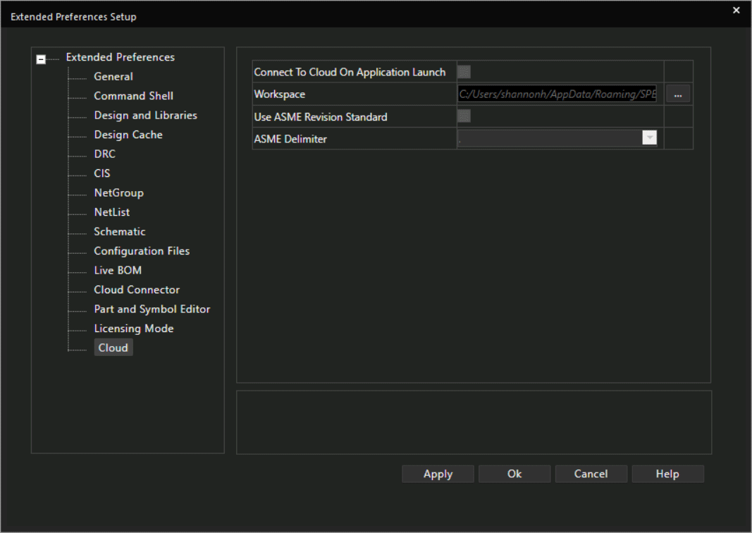
How-ToHow to Enable and Disable Cloud Capabilities in Or...OrCAD X gives you the ability to enable and disable...See More
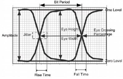
BlogPCB Signal Integrity Simulation: Best PracticesPCB signal integrity simulation is critical for many board designs....See More
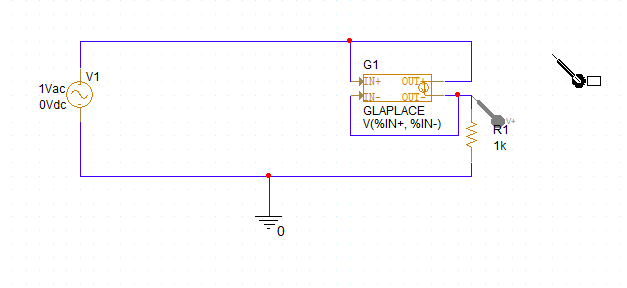
How-ToHow to Model Impedance in PSpice with an Analog Be...Learn how to use an analog behavioral model to simulate...See More
BlogPCB Layer Alignment Design GuidelinesMaster PCB layer alignment and PCB layer design: learn labeling,...See More
On-Demand WebinarsSigrity X: Reimagining Simulation Driven PCB Desig...Join the experts at EMA as we provide an overview...See More
How-ToHow to Quickly Generate Artwork Film RecordsLearn how to generate artwork film records required for a...See More
BlogEssential Differential Pair Routing GuidelinesKnowing and following essential differential pair routing guidelines is critical...See More
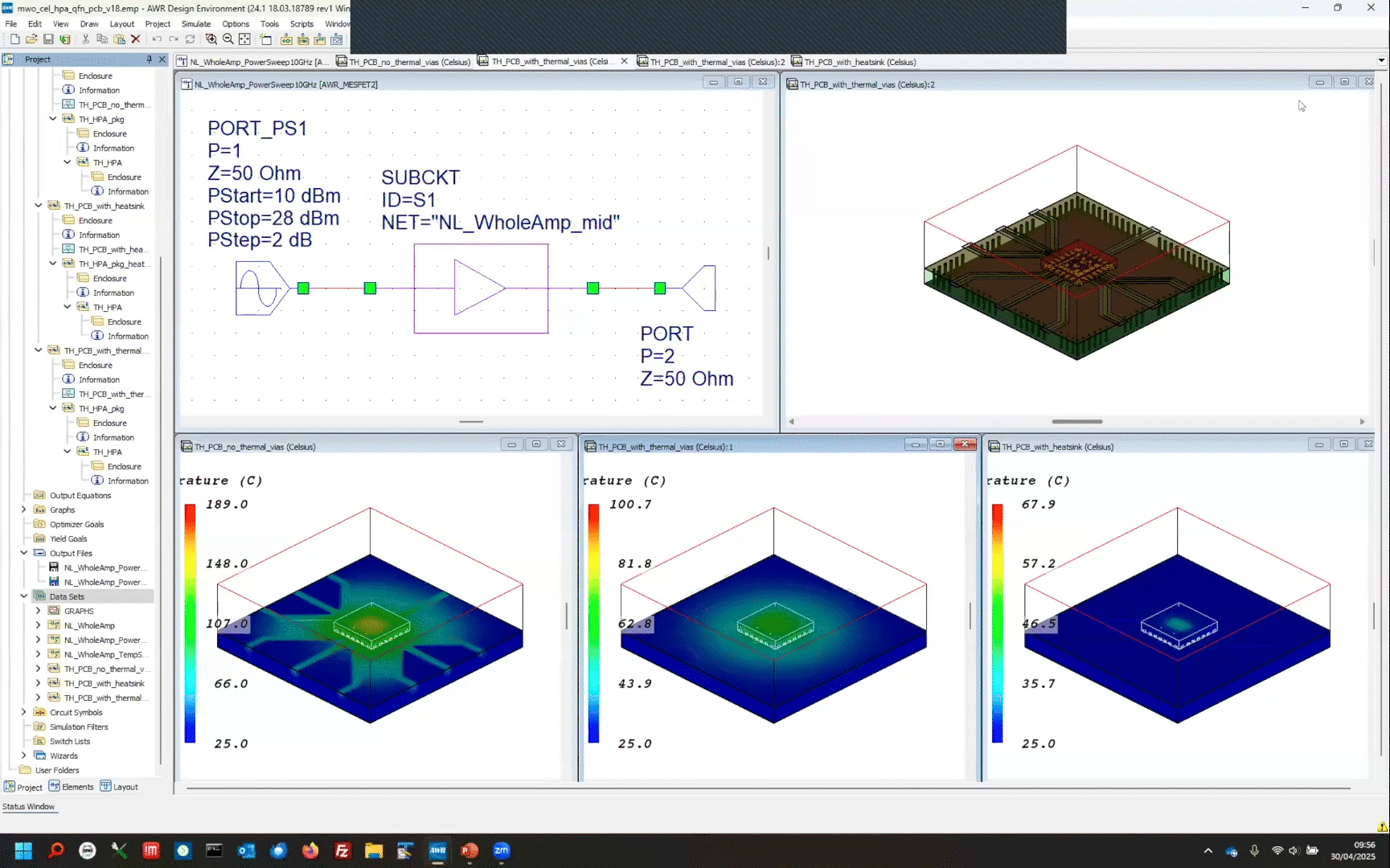
On-Demand WebinarsThermal Implications of Flip-Chip Technology for m...This webinar delves into the thermal and RF performance of...See More