
PCB Design
How to Add Return Path Vias when Routing High-Speed Signals
Learn how to configure and add return path vias when routing high-speed signals with Allegro PCB Designer.
Learn how to configure and add return path vias when routing high-speed signals with Allegro PCB Designer.
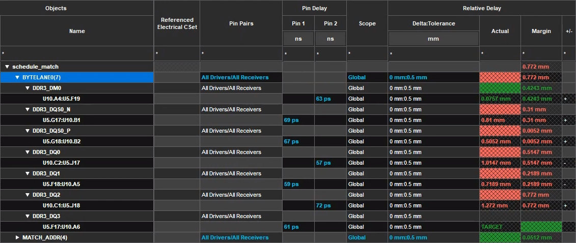
Learn how to incorporate pin delay and z-axis delay into the PCB design to guarantee accurate length matching for high-speed nets in OrCAD.
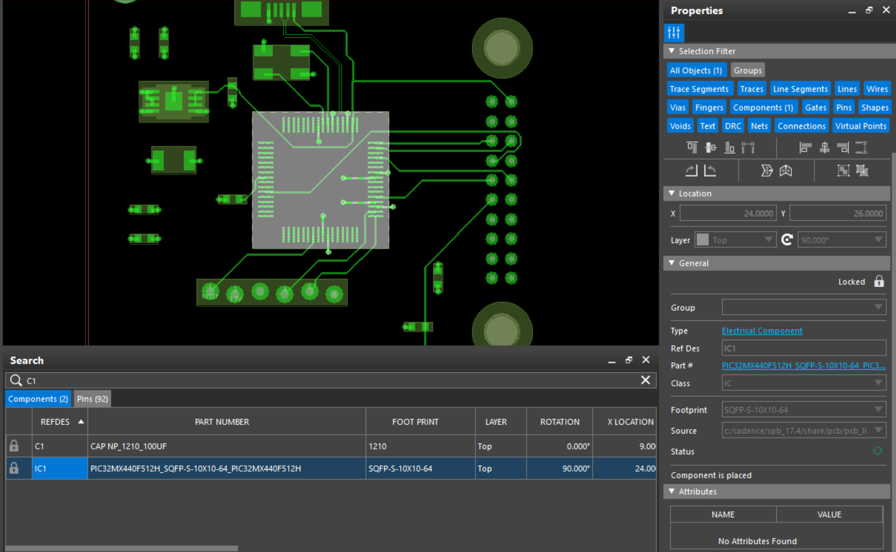
This how-to will teach you how to use the OrCAD/Allegro PCB Free Viewer to intelligently and efficiently review PCB designs.
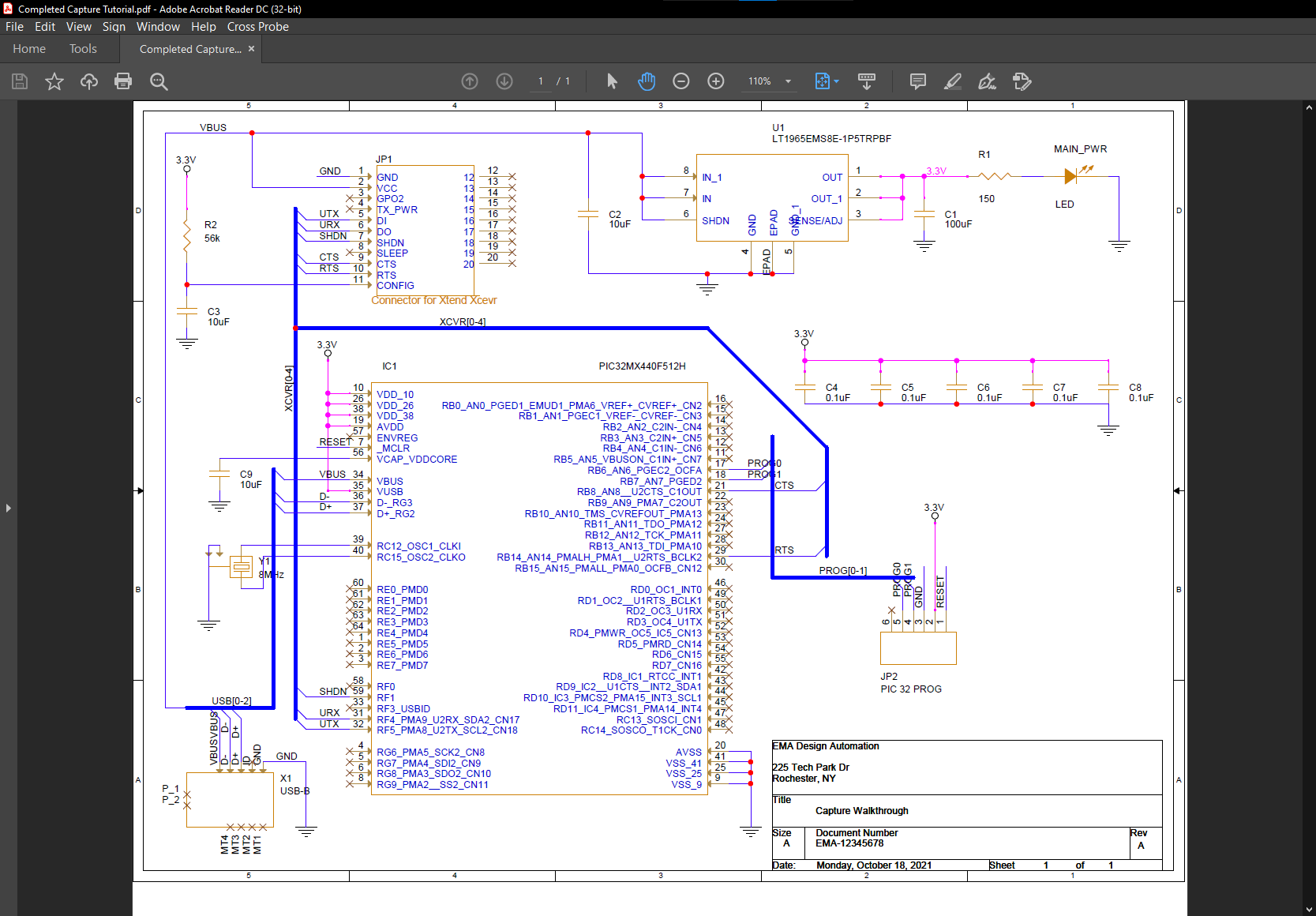
Learn how to use the OrCAD Capture Free Viewer to efficiently and intelligently review schematic designs without tying up a license.
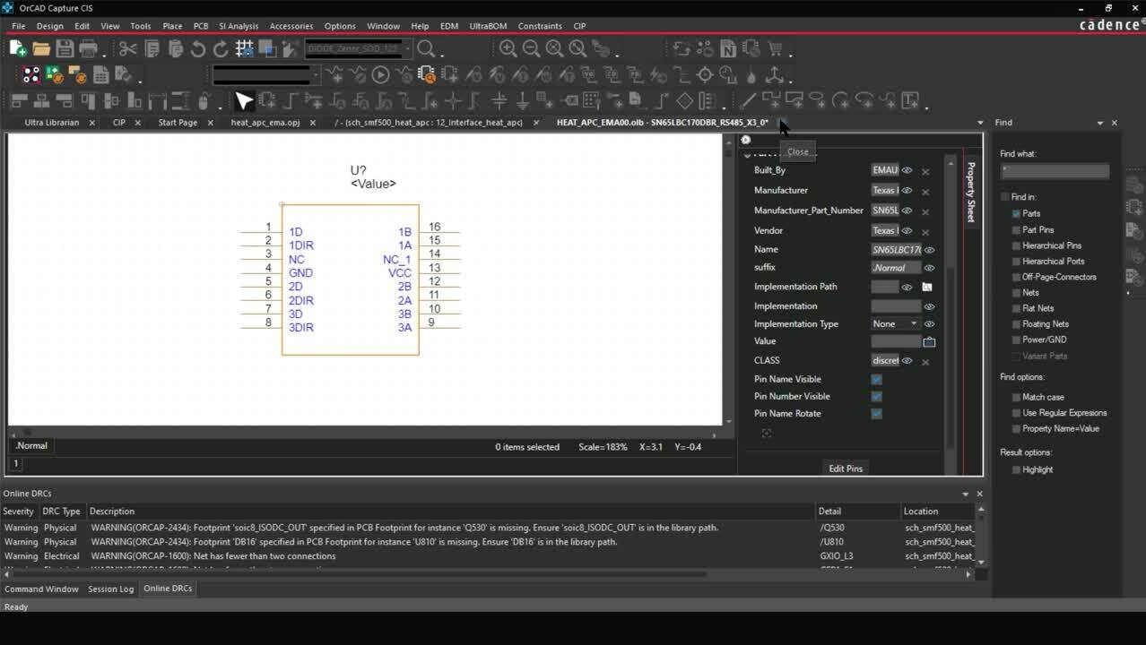
This tutorial provides instructions for the Test Point Back Annotation App in OrCAD to quickly add test points from the PCB to the schematic.
This tutorial provides instructions on how to automatically create fillets or teardrops on traces in OrCAD PCB Designer.
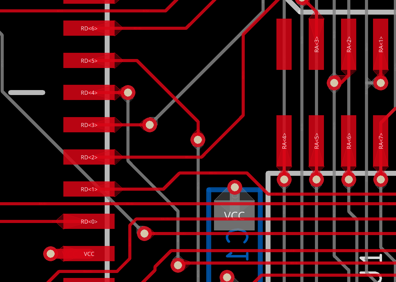
This quick tutorial will provide step-by-step instructions on how to setup XNets for your PCB design using OrCAD Capture and OrCAD PCB Designer.
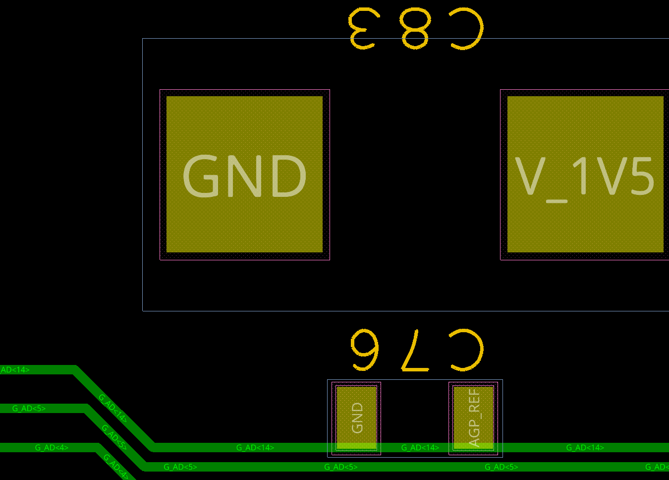
This tutorial provides instructions on how to create soldermask openings for RF signals using Cross Copy in Allegro Productivity Toolbox.
Learn how to use the Mask Generator in Allegro Productivity Toolbox to quickly create oversized masks while preserving the original padstack.
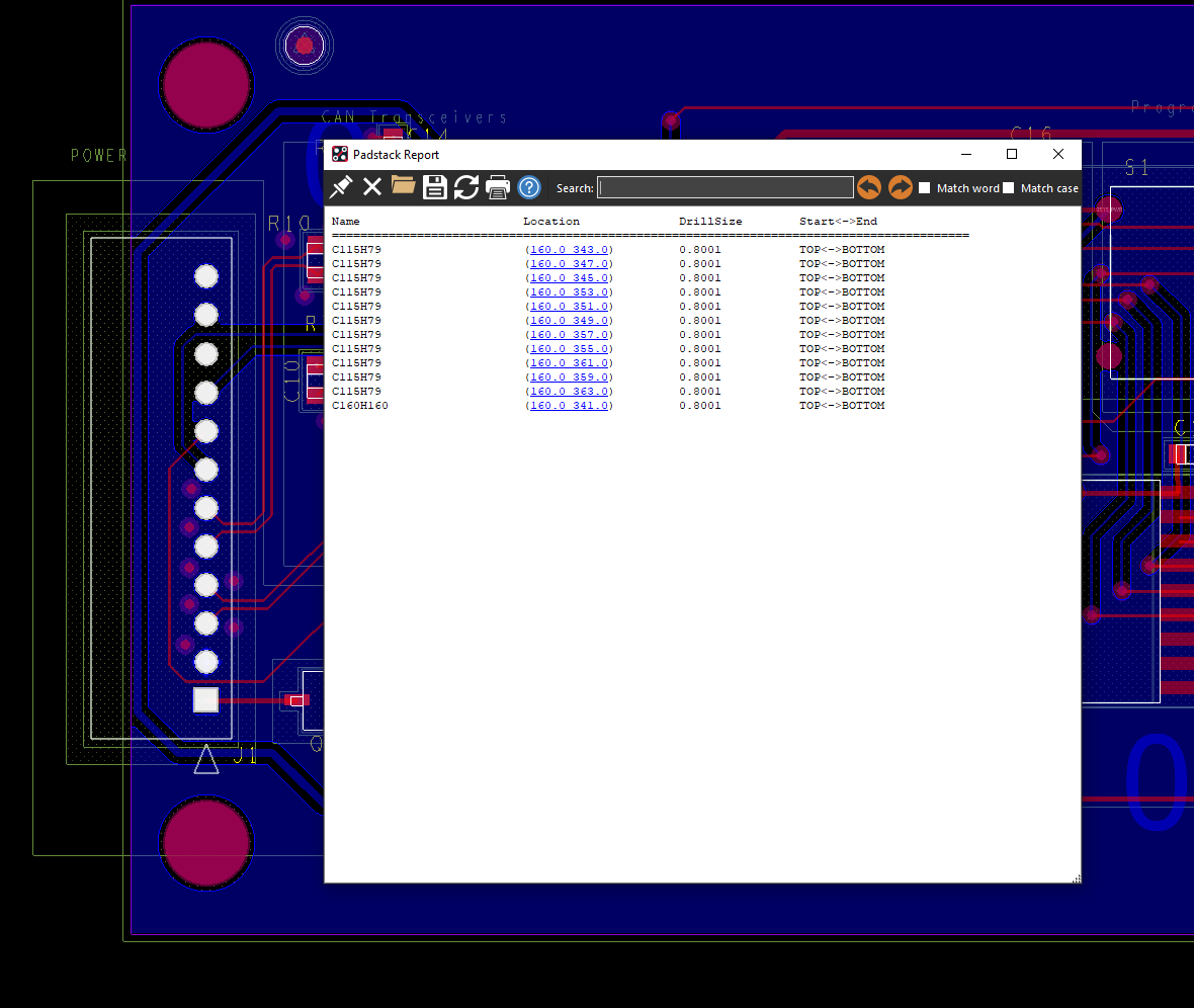
This quick how-to provides instructions on how to find padstacks in the PCB design with Padstack Finder in OrCAD Productivity Toolbox.