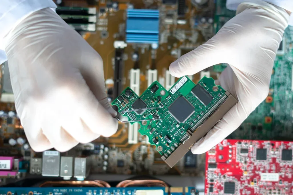
I often receive questions on how to become more confident at designing printed circuit boards. I used to wonder this as well as how I got from knowing nothing about designing boards to being able to work as a freelance PCB design engineer.
What do you need to know? How do you know when a board will work?
After some hard-learned lessons and not-too costly mistakes, I’ve come to realize there are three fundamental principles every hardware maker or engineer can learn to gain more confidence when designing PCBs.
Principle #1 – Design for Manufacturing
Design for Manufacturing (DFM) is essential because if your board cannot be properly manufactured and assembled, it is essentially useless. DFM means your printed circuit board is designed in a way that makes it feasible to build by a PCB manufacturer. In my earlier PCB design days, I never even knew DFM existed until I was in a board fabrication house. I had a bad habit of only paying attention to DFM principles after I had finished my PCB designs.
The truth is, DFM should be considered and followed while designing your printed circuit boards and not afterward. Not paying attention to DFM can lead to board re-spins (which can get quite expensive) and less reliable boards. If you learn and understand DFM principles, you can be confident your design will be fabricated and assembled without issues.
Principle #2 – Power Integrity
The idea of power integrity at its core is maintaining proper levels of voltage and current which all parts on your PCB need to function. But there are more factors that affect power integrity, such as voltage ripple from the power output, signal switching noise / output (SSN/SSO), electromagnetic interference (EMI), and managing the power distribution network (PDN).
Poor power integrity can cause the devices to not operate properly or at all. However, let’s say your PDN provides the right amount of power. Even then, if output voltage ripple from the PDN is too large, you might have devices on your PCB switching signals and sending the wrong data due to involuntary switching caused by that PDN ripple because of ‘ground bounce’.
Learning power integrity can reduce the number of prototypes and production-level board re-spins, saving you significant time and money. Spending 8 hours on a PCB design only to get it manufactured and sent back to realize it doesn’t work properly is frustrating at best.
Let’s say your board comes back and works, but every so often, the memory chips or high-speed circuitry has a glitch in performance. This makes it harder to identify if the issues are a glitch in the firmware or the board itself. It could take several weeks for you or your team to realize the power supply is unreliable and is causing you to fail EMI tests for FCC purposes.
That’s weeks and likely tens of thousands of dollars to solve a problem that could have been detected with better care and analysis during the design phase. I’ve seen it happen at one of my jobs before and the final solution was to replace the power supply and put a few $3 ferrite beads on the board. That’s a painful way to solve a problem. Learning and solving power integrity problems will help to avoid those kinds of time and cost issues with PCB re-spins.
Principle #3 – Signal Integrity
You have a design that can be easily manufactured and put in the time to ensure circuit devices have clean power. You should be fine, right? Not necessarily.
If you’re wanting to do high-speed circuit design, like DDR memory, wireless, and RF designs, you absolutely need to understand signal integrity. The integrity of a signal is paramount to ensure your high-speed or Internet of Things PCB works properly. Otherwise, you can have the same re-spin issues a poor power delivery network can cause.
While the following list is not exhaustive, here are some factors you need to design for when managing signal integrity on your PCB:
- Clock distribution
- Signal paths
- Stubs
- Noise margin
- Transmission lines
- Resistive termination
- Managing signal return paths
The list can go on and feel daunting. Unfortunately, if you want to make reliable, high frequency printed circuit boards (in the hundreds to thousands of Megahertz range), then you need to be good at signal integrity.
Typically, if the transition times are small compared to the trace length (½ of the total time the signal takes to travel along the trace) then you need to consider your PCB as a high-speed circuit. This blog post provides more information on how to identify if your design is high-speed.
Conclusions
Having a thorough understanding of design for manufacturing, power integrity, and signal integrity is essential to be confident when designing PCBs. Once you’ve mastered these three skills, the sky is the limit. You’ll start looking at every PCB differently, be able to re-design and improve them at will, and charge a lot of money for it.