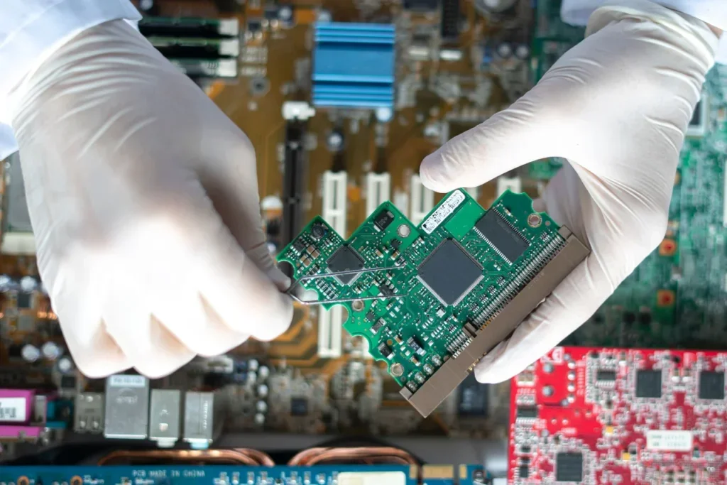
PCB design is becoming increasingly complex as designs and components decrease in size. While you might make design decisions based on common rules of thumb and theories you have learned in school, there are many other factors that could influence your board's performance. Take it from principal engineer, Rich Hartley, from RHartley Enterprises. His focus is to prevent and solve noise, signal integrity problems, and EMI issues through the correct design of circuits and PCBs. During the webinar he presented for PCB2Day, "RF and mixed Signal Layout" he provided information about what RF engineers need during the layout phase. Throughout the webinar, Rick addresses several PCB design myths that cause many common RF design issues. This article will explore five of these myths.
1. Myth: Energy in the circuit originates from the current of voltage.
An often-misconstructed experiment is turning a light bulb on with just two wires and a battery. Many think the voltage and current travel through one wire and back through the second wire between the battery and light bulb, resulting in a lit bulb. Regardless of the AC or DC frequency, this is false. Rather, the energy is found in the electric and magnetic fields themselves.
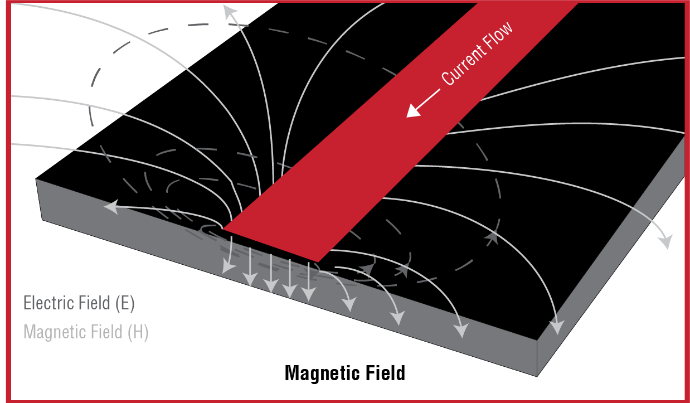
Electric fields start the movement of energy in a circuit, resulting in the excitement of electrons in the copper, thus creating the movement of electrons. The combination of movements generates a magnetic field. Essentially, the fields ARE the energy source because they generate the voltage and current.
2. Myth: Energy travels in copper elements.
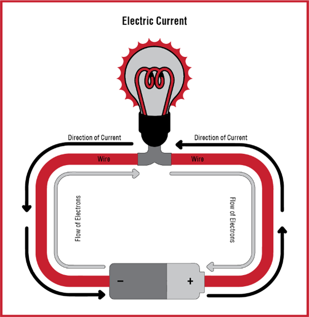
Some say energy travels down the copper trace or wire, excites the load, then travels back through the plane to the source. Energy travels in one direction only, as a wave down the transmission line (usually a pair of wires or conductors). As it moves, it moves electrons (current flow) in the trace and plane, simultaneously in both directions. The movement of electrons carries the charge. The copper traces and planes are only present to help steer energy from point A to point B with low impedance paths.
3. Myth: A piece of wire has inductance.
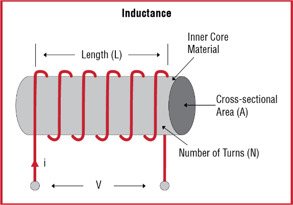
This myth is partially true, as a piece of wire has partial inductance. However, for the inductance to be accurately defined, there must be a complete circuit consisting of a copper trace and plane combination. To calculate inductance, you will need: two wires with a defined spacing between them, a defined gauge and length, and known twists in the pair.
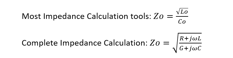
4. Myth: Regular impedance calculators are suitable for RF design.
Impedance is defined as how well energy moves through the material without losses. The PCB material impacts conductance because the energy travels in the space between the copper and therefore through the board material. Most regular impedance (Zo) calculators take the square root of inductance (L) divided by capacitance (C). This means they ignore the resistance (R) and conductance (G) in the complete impedance calculation. When it comes to HF, VHF Analog, or High-Speed Digital circuits, the resistance and conductance are highly important and must be accounted for. Therefore, this myth is false and a quality tool like a field solver is a must in RF design.
5. Myth: You can determine the inductance in a single via.
False. It is impossible to determine the inductance of a single via. To determine inductance, vias should come in pairs– one for power and one for ground. Inductance is a proximity event rather than a size event. By moving vias closer together, inductance can decrease by 60% when correctly placed besides decoupling caps. This is in stark contrast to increasing the via size, which would reduce inductance a mere 12-14%.
Knowledge of PCB design is evolving as quickly as the technology we use in our circuits. With RF signal requirements increasing, relying on theory and rules of thumb will not always work and can lead to costly mistakes. If you would like to learn more about various electronics design and manufacturing topics, sure to lookout for more webinars from PCB2Day, who consistently feature knowledgeable and experienced speakers like Rick. In addition, visit our free resources page which contains various PCB design resources such as whitepapers, webinars, blog posts, and more.