With everything from your cell phone to your teddy bear sending and receiving wireless signals, RF interference is a growing concern. Even if you aren’t transmitting, you may have RF sensitive circuits you need to protect—almost every wire becomes an antenna or receiver and the signals they can receive or transmit can degrade overall performance. This is true for all products, no matter how small or minor they might be.
Since this problem isn’t going away anytime soon, it is critical to have a good understanding of how our design parameters can affect RF interference levels.
After a conversation with Orlen Bates, an EMA Field Applications Engineer with 44 years’ experience (his first RF circuit was hand taping and Xacto-knife trimming), we have come up with a list of 5 Design Tips to help prevent RF interference in your designs.
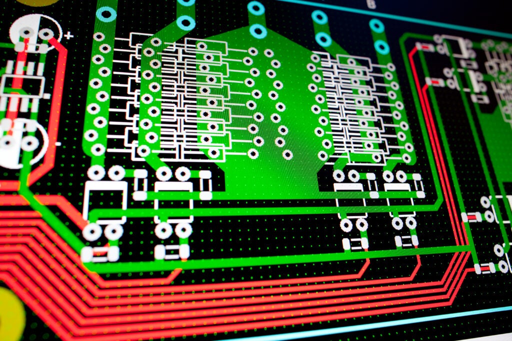
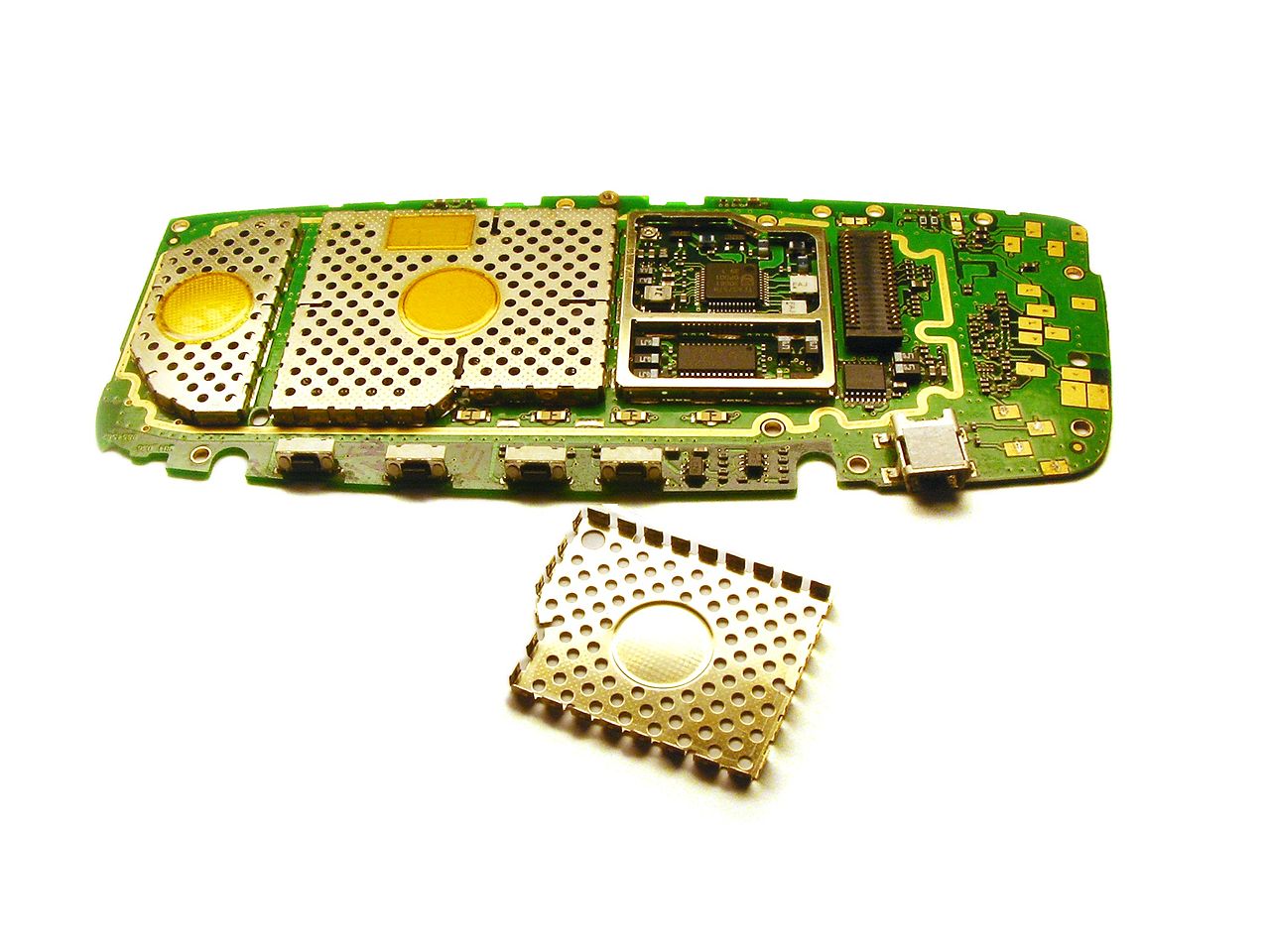
1. Moats aren’t only used on castles. Well, no we don’t mean a literal moat. Shielding, or what we lovingly refer to as a “moat”, is important to add to critical sections of the board to prevent interference, or to prevent interference from other portions of the board, affecting sensitive circuits. The moat is that line in the PCB that keeps RF on one side and other signals on their side. Many RF vendors define signal quality with a term called the signal-to-noise ratio (SNR). The SNR is the difference between the received signal and the background noise level. The “moat” must encompass all RF parts/circuitry and is the land pattern for the fence or metal can.
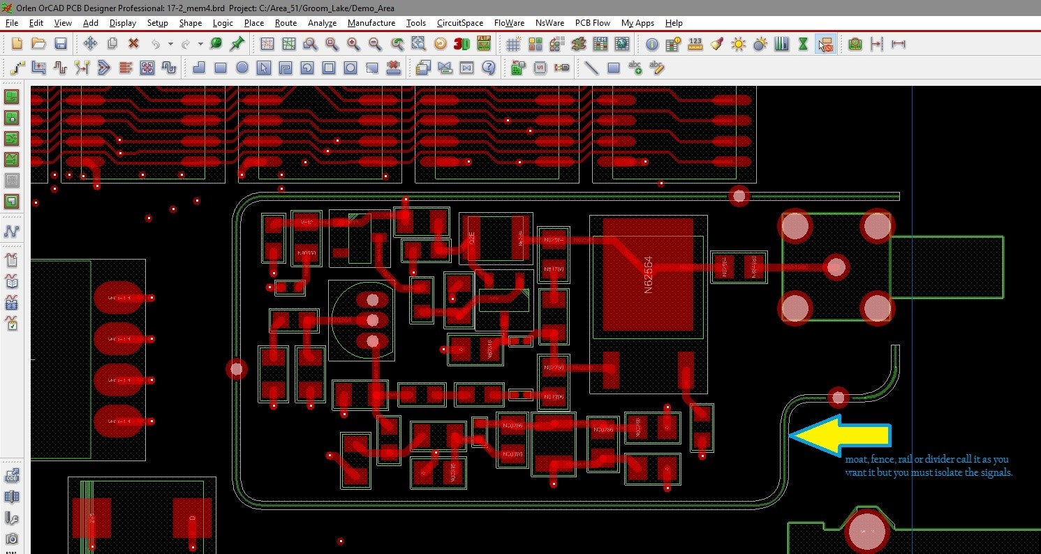
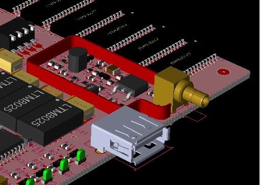
Image 2: The moat with a fence installed. Moats are used to help isolate outside interference of any kind.
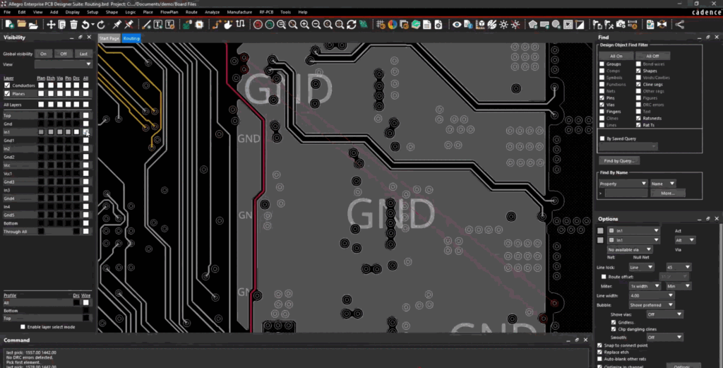
2. Ground location matters. You wouldn’t design a lightning rod to go through your castle; you would want it to take the shortest path to ground so it has the least likelihood to catch anything on fire. This is the same with PCB Design. Ground location is the first line of defense when it comes combating RF interference. Shielding on the layer RF ground plane should be placed directly below component layer. This paired with vias will allow the noises picked up to go straight to the RF ground plane. This will help to minimize noise, since we cannot truly eliminate it.
3. Vias help drain the moat. Vias are the drain hole to the RF ground plane below. They are the collecting points and in this instance, the more the merrier. To reference our lighting rod analogy again, the lightning rod does you no good if it’s not a reliable connection to the RF Ground Plane—it must be tied down into the ground. This is where vias come in, the noise goes down into the RF Ground via the via. Via arrays need to be along the “moat” down to RF ground plane (micro vias work best).
4. The only way one can leave is at the “draw bridge.” RF connectors (the draw bridge) by design must have an opening in the fence or metal can. Just like with our castle, to be truly secure, we need to control where the exit is. Controlling the direction of noise is equally important when you are trying to control noise issues. By providing only one opening, you control the direction of the noise as well as prevent it from going in multiple directions. The RF Connector is normally the only opening to the outside area around the RF Circuit.
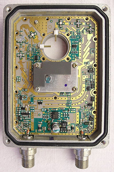
5. Simplicity is your friend. Having to use irregular shapes can drive costs up. Try to make your layouts to adhere to standard “moat” shapes like rectangles or square—bending metal takes time and cost money.
In conclusion
When it comes to limiting RF interference, there are numerous factors to consider and be aware of. If the signal is not properly controlled, it can lead to costly respins, wasted time, not to mention a whole other host of operation, safety, and health issues. The tips above are designed to help you mitigate some RF interference through PCB design.

