Two of the most compelling forces driving much of our technology, Miniaturization and Performance are not new. In fact, one could say they have appeared within every product spec and design document in some form or another since the terms were coined. Fundamentally, this is great and has enabled capability and portability with products in virtually every hardware sector. This will (and should) continue.
In the area of miniaturization, both board and package are transforming as technologies like rigid-flex, blind/buried vias, and multi-die packages continue to move from fringe to mainstream. Furthermore, performance improvements maintain the well-known doubling trajectory and is propelled forward by orders of magnitude in speed while increasing efficiency and extending battery life. Often these gains are only continually achievable by reducing the voltage swing to under a volt.
As Miniaturization and Performance drives our devices to new heights and applications, the effects of these requirements are visible throughout the design process and nowhere is this drive for smaller, faster, cheaper, more noticeable than in the area of power.
Power Demands Outpacing Supply
To comprehend the extent of the Power Delivery Network (PDN) transformation, consider the following. Design requirements associated with power delivery have become substantially more complex with many IC’s requiring power to be supplied at multiple voltage levels. Frequently those levels are near or below a single volt, contracting virtually every threshold and reducing margins to mere millivolts. Simultaneously, the demand for current has skyrocketed in some product areas, made obvious by the extent to which we now account for adequate cooling.
In addition to these increased electrical demands, the PDN must also be more responsive, capable of supplying the instantaneous current demands of high-speed signaling. While all this may suggest a more robust PDN is needed, as many new products reach manufacturing, often the opposite is true. Not surprisingly, the miniaturization effort has had a consolidating effect on the physical hardware, frequently bringing high current ICs closer together. Advances in device packaging have contributed as well. Pin counts can easily exceed a thousand on a single package and mainstream spacing under a millimeter all contribute to the same reality, PDN is comprised of less copper in today’s PCB than it was just a few years ago.
Getting Control of Your PDN from the Start
Recognizing this is a trajectory where power delivery WILL become problematic and conceding that for some designs it already has, progressive product development teams are looking to Power Integrity simulation for answers. We’ll see in subsequent articles several elaborate interactions attributable to the power system, such as complications with “the return path” and the ability to shield and control EMI, but first we need to ensure adequate capacity and effective distribution. Commonly referred to as the “DC” branch of Power Integrity, its primary task is to guarantee sufficient current sources at a steady voltage. The PDN must provide a conductive path such that, current leaving the supply does not experience so much resistive loss the voltage can’t be maintained when the device is drawing its maximum current. It is essentially an Ohm’s law problem.
By understanding a device’s operating voltage and maximum current draw are defined by its specification, we quickly see the PDN resistance is the only design element where a product team has any control. Signal Integrity has taught us the physics associated with current flow and electrical conduction is very predictable. We recall that with knowledge of the materials and conductor geometry, accurate/predictive characterization of electrical behavior can be determined. Mathematically, Power Integrity, aka PI or Power Delivery Network analysis, has many similarities with its signal integrity roots.
What is strikingly different however, is the actual copper under examination and the current being conducted. Contrast the wide, copper-flooded areas (to include entire planes) associated with power routing with the thin line of a signal trace and we’d naturally expect the resistance to current flow would be much different. Likewise, consider the short bursts of current we see when digital signals switch, first in one direction and then the other, and compare that to the steady drain, source to load, we see for power signals. Therefore, the physics of conduction are the same, but the signals being conducted are very different, requiring different types of analysis and methodologies to meet our power delivery goals and demands.
DC AKA Distribution and Capacity
As previously referenced, our DC goals for power delivery or PDN can be broadly defined as distribution and capacity. Distribution implies all devices, even those farthest from the supply, have access to adequate current, at the defined voltage. Similarly, under extreme demand, capacity ensures the power system can maintain that voltage even when current draw reaches its allowable maximum. If the voltage supplied at every device doesn’t droop below the acceptable value, we can therefore have great confidence that even if each device needs to draw it’s most aggressive current, the power delivery network is capable of distributing adequate current to all devices.
Solving for V
The DC capability associated with Power Delivery Network analysis, only requires two things: an accounting of load and resistance. An accounting of load is simply how many devices are being supplied and how much current does each device require. Cumulatively, this the “I” in our Ohm’s law (V=IxR) reference. Resistance, or “R”. We know from previous discussion simulators routinely calculate resistance, even Impedance (“complex resistance”), given only the materials and geometry contained in their CAD databases; this is exactly the case with Power Integrity.
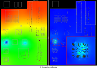
Often accessible directly from within the PCB CAD tools, PI simulators can readily identify conditions where a chip could become “power starved”, but it doesn’t stop there. Because the tools create a model of the board, all the properties (voltage, current and resistance) can be displayed as color-coded overlays directly on the board’s etch. This enables both visualization of a problem and an environment where corrections can be made in the native CAD tool and be reflected in the design file. While not specifically addressing Power DC issues (one of distribution/capacity), these additional overlays are useful for identifying other concerns associated with power as well. Areas of high current density which could result in both EMI defects and reliability issues, can be easily detected and prevented as the simulators produce an intuitive, visual model of the power network.
Moving Up A level of Abstraction
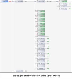
Power Integrity, DC simulators exist from a number of vendors and have universally proven to be quite accurate. This is largely due to the extensive studies on copper conduction for the RF and high-speed digital industries. While traditionally this type of analysis has been done at the Layout and routing phase of the PCB, it has become increasingly apparent analysis needs to move up a level of abstraction to incorporate earlier system-level, power budgeting and inspection.
In this analysis, for example a DC-to-DC convertor’s dual role would be recognized, both as a load to the main supply net and the origin (supply) of the power net produced at its output. Leveraging the PCB model as a SPICE model, external circuit elements like switches, resistors, and transistors can be included, allowing simulation of the system itself. Extending system-level checks to include device SPICE models extends both the checking and display capability beyond individual nets to the system. This enables “sizing” and capacity checks to encompass device selection and verification in addition to the checks performed on the etch alone.
Power Delivery Network Analysis: Pressure is Not Going Away
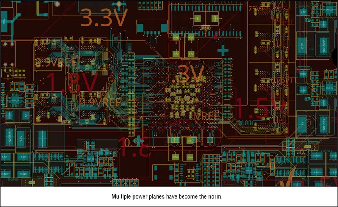
Although we can’t predict what technologies will drive product direction in any hardware sector, it’s safe to say there is little desire for bigger, slower, less efficient anything. Therefore, both Miniaturization and Performance will continue to be prominent, and they have their sights on all that “extra power plane copper”.
Will you be ready? Continue reading this series to learn more about incorporating power delivery network analysis into your design process with Jernberg PI #3: The Case of the Unresponsive PDN.
Contact us for more information on how Sigrity can be used to analyze signal integrity and power integrity for PCB Designers.