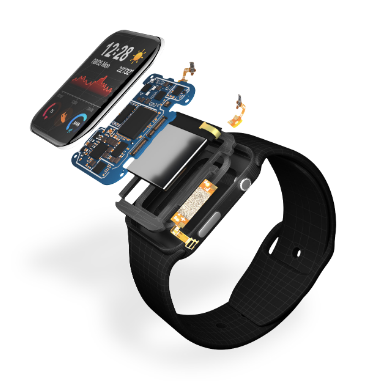
What is the future of high-speed data transfer? If the present is any indication, it will be astronomical. In 2023, NASA set the world record by transferring 4.8 TB of HD video from a low earth orbit (LEO) satellite to Earth at a blazing 200 Gbps. This feat was accomplished via infrared laser using optical technology. Yet, optical communications employ circuit boards just as RF communications systems do.
For RF, which extends from 20 kHz–the low-end of the human audible range–to 300 GHz, high-speed PCB design typically refers to boards where the highest signal frequency is at least 50 MHz. This general estimate is often seen as the level at which signal integrity for high-speed design becomes an important consideration. Whether you employ this rule-of-thumb metric or a more accurate calculation based on trace lengths and board materials, it is important to know the signal integrity problems that can adversely affect your PCB’s performance and the best way to mitigate these issues.
Addressing Signal Integrity for High-Speed Design
Successfully addressing signal integrity issues is critical when designing high-speed circuit boards. Doing so necessitates an understanding of common issues, their impact, and winning mitigation techniques, as listed below.
It is not uncommon for a design to have multiple SI issues to address with many of the concerns above overlapping. Therefore, when choosing a solution for signal integrity in high-speed design you should look to the best simulation software tools, which possess multiple features and capabilities.
Signal Integrity for High-Speed Design
Elements like beginning with accurate CAD models must be addressed to ensure successful high-speed design. But prior to employing any signal integrity solutions, it is helpful to start with a definition of what high-speed design actually means:
High-Speed on a PCB refers to the existence of signal propagation conditions that make it necessary to tailor PCB design characteristics such that a signal’s electrical attributes are minimally altered as it traverses the circuit board. These conditions include type of signal, signal frequency, signal path, trace length and board material.
Effectively, your board should be considered high-speed if any trace is considered a transmission line, which may be the case if the following inequality is not satisfied.
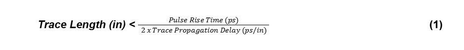
Typically, digital pulses have faster transition times than analog signals, and impedance, which is a major determinant of propagation delay, is lower for surface signals as opposed to on internal layers with the same dielectric material. It is possible to experience some of the adverse effects associated with high-speed signal transmission as lengths shorter than defined by Eq. (1). Consequently, it is recommended to choose your trace length based on wavelength (𝝀), as shown in Eq. (2).

In Eq. (2) above, the propagation speed, 𝝼, varies according to the board material dielectric and whether the signal is on an external or internal trace. NOTE: For surface signals, propagation speed can be estimated to be approximately 85 ps/in.
Designing for Maximum High-Speed SI
As explained in the previous section, several factors determine whether your board is considered high-speed. This determination is the first of several guidelines to follow to maximize the performance of your PCB.
By employing good PCB layout design best practices and following the guidelines above, you can ensure your board will deliver the best quality signal propagation and meet your design objectives. However, it is important to implement the best software solution for your project and situation. The best option to satisfy this requirement is to partner with the industry leader in providing software and support for PCB design.
EMA Design Automation is a leading provider of the resources that engineers rely on to accelerate innovation. We provide solutions that include PCB design and analysis packages, custom integration software, engineering expertise, and a comprehensive academy of learning and training materials, which enable you to create more efficiently. For more information on how to maximize signal integrity for high-speed design and how we can help you or your team innovate faster, contact us.