A thoughtfully-made, preplanned PCB layout can make a board operate more reliably, and ensure better performance. This guide provides important PCB design layout guidelines, touching on design rules, reliability factors, functionality, and manufacturability. By following best practices, designers can achieve successful layouts that minimize errors and improve efficiency.
Essential PCB Design Layout Best Practices
PCB design is typically partitioned into two major stages: Schematic design and PCB Layout design. Although distinct, these stages are not mutually exclusive. In fact, the best layout design begins with a thoroughly reviewed and verified schematic design, and proceeds by employing best practices, as listed below, to maximize the effectiveness of good PCB design layout guidelines.
PCB Design Rule Guidelines
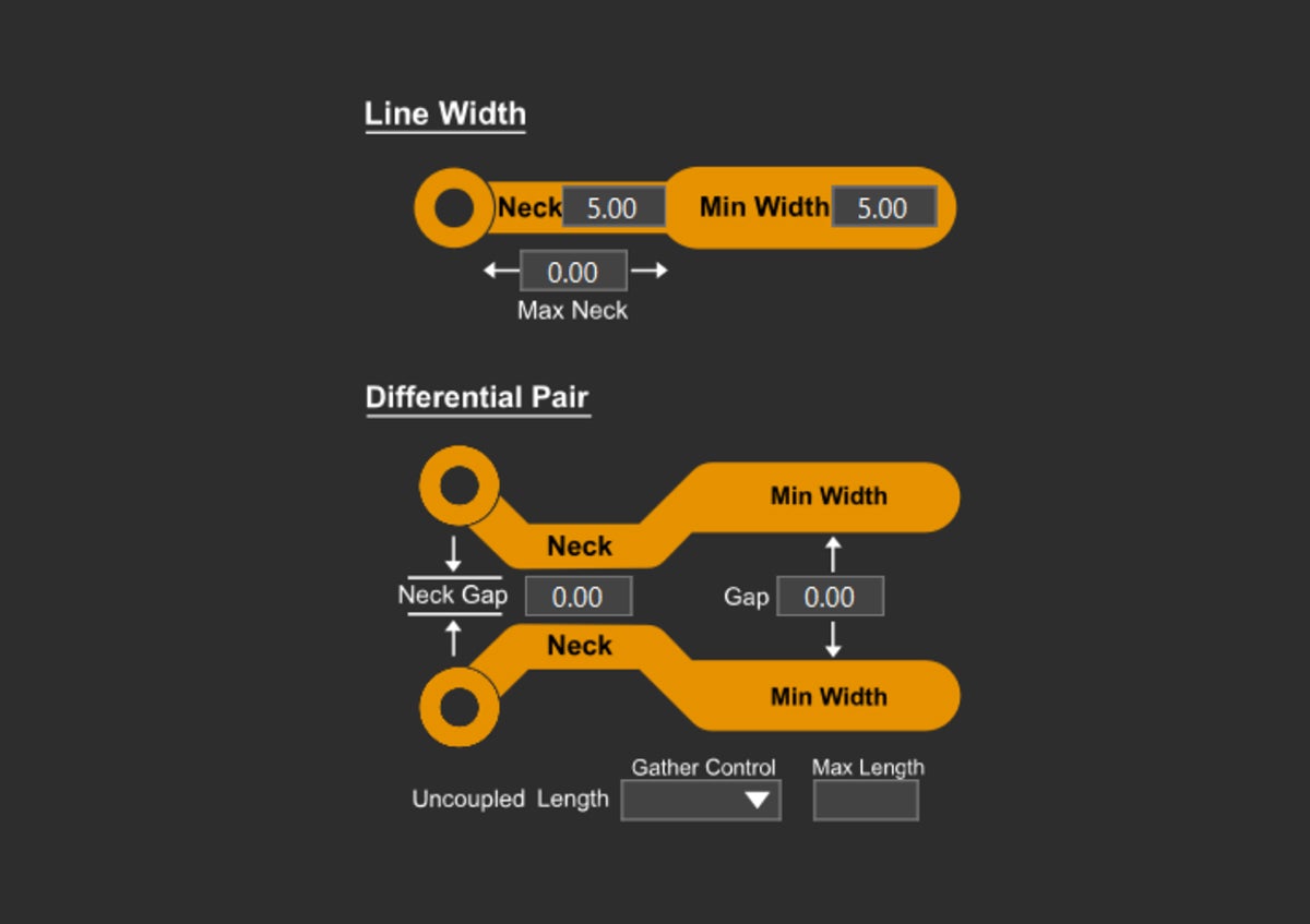
- Minimum Trace Widths and Spacing: Calculate minimum trace widths using guidelines like those provided in IPC-2221, considering factors such as current capacity, permissible temperature rise, and copper thickness
- Via Size and Placement: Define via sizes to meet the electrical and thermal requirements and ensure that vias align with manufacturer capabilities.
- Component Clearances: Avoid component crowding to ensure easy soldering, inspection, and troubleshooting.
- Layer Stack-Up Requirements: Set up a layer stack-up that meets signal integrity requirements, often consisting of ground and power planes to control impedance and reduce noise. Utilize symmetric stack-ups to minimize warping during fabrication. Incorporate ground planes adjacent to signal layers to provide return paths and reduce electromagnetic emissions.
Important Reliability Considerations
- Thermal Management: Intelligent thermal management prevents overheating and prolongs component life. Key layout guidelines include placing high-power components away from sensitive components, and using large copper pours or dedicated heatsinks to help dissipate heat.
- Controlled Impedance: More important in high-frequency circuits, controlled impedance reduces signal loss and reflections, maintaining signal integrity. Use controlled impedance routing for signals like DDR, USB, HDMI, or Ethernet. Ground and power planes in multi-layered PCBs help control impedance by maintaining a consistent dielectric thickness between layers.
- Electromagnetic Interference (EMI) Mitigation: EMI and electromagnetic compatibility (EMC) can be managed with direct signal paths and avoiding right-angle turns in traces. Ground planes and strategic shielding around sensitive analog sections also contribute to EMI and EMC control.
Component Placement Guidelines
- Group Components: Place components based on their functional relationships. For example, group analog and digital sections separately to avoid interference.
- Ensure Stable Power Delivery: Position critical components, such as processors or oscillators, near power sources to minimize power and ground loop areas. Place decoupling capacitors as close as possible to the power pins to stabilize power delivery. Ensure that decoupling capacitors have low-inductance paths to ground by using wide traces or vias directly to ground planes. For high-frequency decoupling, use multiple capacitors of different values in parallel to filter a wider range of frequencies.
- Optimize the Power Delivery Network: Keep power supply components near the power inlet, creating a direct and low-resistance path to the power pins of critical ICs. This placement minimizes voltage drops and improves power integrity.
- Consider the Assembly Process: Avoid placing components near the edges of the PCB or in positions that make automatic assembly challenging. Standard spacing guidelines for pick-and-place machines should be followed to minimize assembly errors.
PCB Layout Guidelines
- Minimize Layer Count: Using fewer layers can reduce cost but may also increase complexity. Therefore, care must be taken not to compromise trace width, spacing, or signal integrity.
- Separate Planes for High Power and Low Power: Keep high-power and low-power planes separate to minimize noise coupling. Sensitive analog circuits benefit from dedicated ground planes that are isolated from noisy digital sections.
- Use Multiple Vias for High Current Paths: When connecting power or ground planes across layers, use multiple vias to handle higher currents without causing excessive temperature rise. Place vias in an array or grid pattern to evenly distribute current and heat.
- Use Thermal Reliefs on Vias: Thermal relief patterns around vias prevent heat concentration at the connection points, which is critical during soldering. This patterning reduces the thermal mass that needs to be heated, aiding in efficient soldering and reducing thermal stress.
Key DFMA Layout Guidelines
- Clearances for Automated Assembly: Consider spacing requirements for automated soldering and inspection equipment. Keeping components accessible reduces assembly errors and improves yield. Provide adequate silkscreen labeling for component identification during assembly and troubleshooting.
- Test Points for In-Circuit Testing (ICT): Including test points for ICT allows for effective testing during production, enabling quality control and quick identification of issues. Test points should be easily accessible and free from obstructions by other components. Consider using boundary-scan or JTAG interfaces for complex ICs.
PCB Layout Verification Guidelines
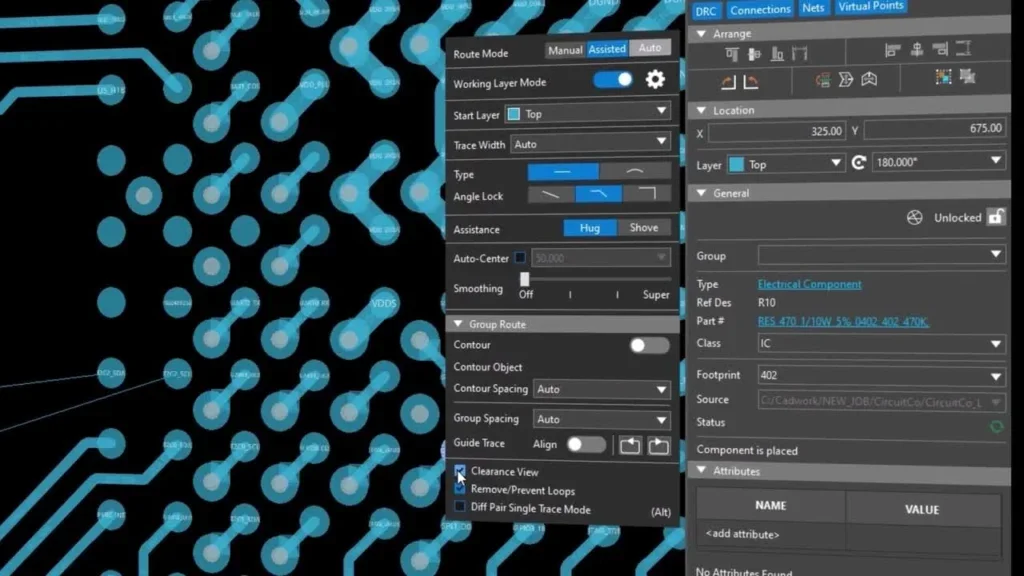
Effective PCB design layout guidelines are incomplete without considering the verification of your board, prior to manufacturing. The best PCB layout software tools include functionality and capabilities that specifically address this often overlooked requirement for PCB design optimization. Using Computer-Aided Design (CAD) tools like Cadence OrCAD with advanced X layout features, designers can incorporate real-time design rule checks (DRC) to flag any violations early in the layout process, easily collaborate for complex designs and integrate with industry leading software simulation programs to initiate and facilitate an optimal design and development process.
Adhering to PCB design layout guidelines and using effective software tools are essential for achieving board layout efficiency and creating reliable and manufacturable boards. However, it can be challenging to optimize your PCBA design workflow situation, which may require selecting the best PCB design program and/or employing the most useful simulation tool. The best option is to look to an industry leader in providing engineers and teams with the best software and support that meets their requirements and scales with their growth, EMA Automation.
EMA Design Automation is a leading provider of the resources that engineers rely on to accelerate innovation. We provide solutions that include PCB design and analysis packages, custom integration software, engineering expertise, and a comprehensive academy of learning and training materials, which enable you to create more efficiently. For more information on how to best incorporate PCB design layout guidelines and how we can help you or your team innovate faster, contact us.