EMA Resources

Blog

Home > EMA Resources > Blog > Most Effective PCB Analysis Methods

Most Effective PCB Analysis Methods

The effectiveness of PCB analysis methods can seem magical.

The effectiveness of PCB analysis methods can seem magical.

Designing electronic circuit boards that satisfy the needs of many stakeholders while producing a reliable PCB that achieves functional and operational intent is a complex task that necessitates the use of PCB analysis software. Although the effectiveness of these tools can seem magical, they are based on sound engineering principles. Understanding these PCB analysis methods will help you select the best analysis tools and leverage them properly.

PCB Analysis Methods and Design Techniques

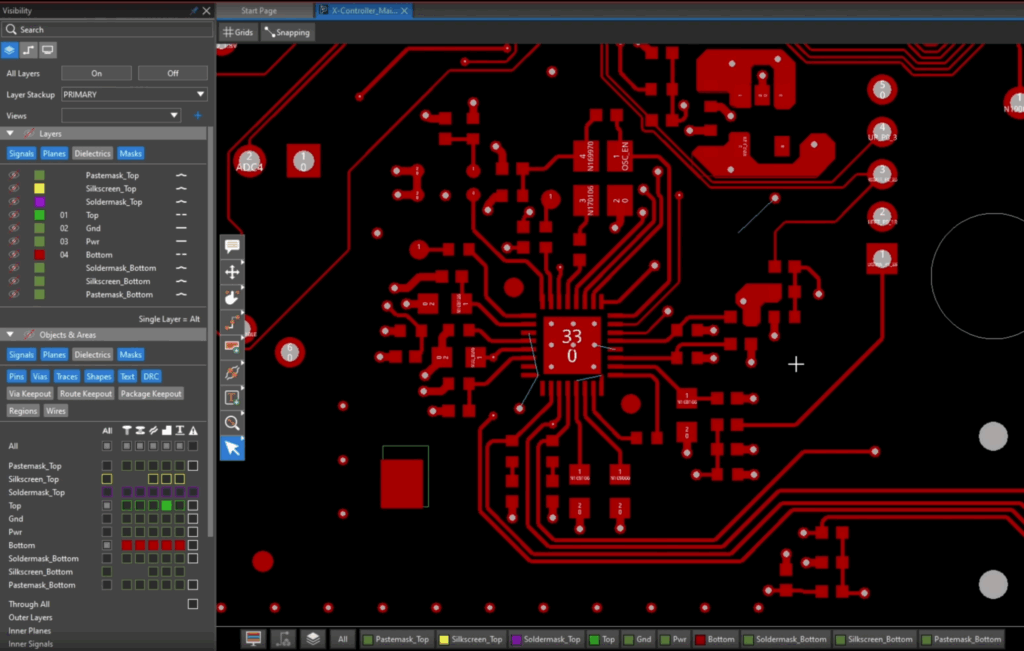
Employing PCB EDA tools is often dominated by traversing the steep learning curve to understand how to use the UI efficiently. However, the true quality measure of a PCB synthesis, simulation, or verification program lies in the underlying engineering methods and techniques that drive analytical design tools, as listed below.

Electronic PCB Analysis Methods
Analysis Method Purpose Common PCB Design Application(s)
Nodal and Loop (Mesh) Analyses To determine unknown voltages and currents; typically applying Kirchoff’s current and voltage laws (KCL, KVL) IR voltage drop analysis
Transmission Line Modeling Provide standard impedance models for analyzing effects on signal flow  Impedance analysis
Fourier Analyses To convert periodic time signals into frequency representations for simpler analysis Signal integrity analysis
Laplace Analyses To convert complex time signals to algebraic frequency representations for simpler analysis High frequency RF simulation analysis
Scattering (S) Parameter Analyses Provides a frequency model for analysis of RF circuit behavior RF simulation  
Superposition Used to evaluate the effects of multiple sources within a circuit independently. Thermal analysis
Finite Element Analysis Enables discrete interval analysis of electrical parameters. CFD analysis
Bode Plot Analysis Provide an ideal target to optimize filter design  EMI and EMC analysis
Z Transform Analysis To convert discrete time signals for digital system analysis   Timing circuit design

The applications listed above are not exhaustive. In fact, most of the PCB analysis methods and techniques in the table are used in various EDA software tools. It is important to note tools that target a particular analysis type will employ component, circuit, and system models designed to maximally leverage the mathematical prowess of the underlying analysis method. 

Optimizing PCB Analysis Method Usage

The keys to effective and efficient PCB design at every stage are to know and follow best practices and equip yourself with the best software tools that allow you to do so. This is true for optimizing PCB analysis method usage as well. Implementing the guidelines below will help you achieve this goal.

PCB Analysis Method Implementation Guidelines

  • Understand PCB analysis methods and how they are implemented.
    The first step to selecting the best tool is to understand the underlying principles and techniques on which the program is built as it determines its effectiveness.
  • Choose a PCB CAD design platform that meets your design needs.
    PCB CAD programs are not created equal. Consequently, it is important to elevate important factors such as capabilities, usability, and scalability in order to select the platform that best aligns with your particular design needs.
  • Follow best practices for schematic and PCB layout design.
    The best practice for PCB design is to create a strong foundational design by following a good schematic design checklist and PCB layout guidelines. 
  • Employ PCB support software for additional analysis capabilities.
    Depending on your design platform and specific project requirements, you will likely need PCB support software to provide additional simulation and analysis capabilities.
  • Select the best simulation and verification tools.
    To compete in today’s electronics industry, it is essential that you leverage the best software tools. Consequently, it is important to know how to choose the right simulation software that meets your needs today and will continue to do so as your needs evolve. 

Following the guidelines above will greatly aid you in selecting the best software tools for your specific needs. However, researching and evaluating the options can be challenging. The best option is to rely on an industry leader to supply engineers with the software and support that satisfies their requirements.  

EMA Design Automation is a leading provider of the resources that engineers rely on to accelerate innovation. We provide solutions that include PCB design and analysis packages, custom integration software, engineering expertise, and a comprehensive academy of learning and training materials, which enable you to create more efficiently. For more information on how to best employ PCB analysis methods and how we can help you or your team innovate faster, contact us.

LinkedIn
Email

Table of Contents

Get Content Like This Delivered Directly to Your Inbox

Related Resources

EMA Design Automation