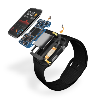
The PCB design software you use directly impacts the efficiency, accuracy, and success of your electronic product development. With advanced features like supply chain resilient component selection, auto-interactive routing, and signal integrity analysis, high-quality software ensures error-free and optimized circuit layouts. Additionally, some design programs enhance team collaboration, deliver seamless data transfer and help facilitate efficient manufacturing, reducing production errors and costs.
Optimizing your circuit design and development depends on how well your software meets your particular project requirements. Achieving this goal necessitates that you are aware of available capabilities. To aid you, we have compiled a list of top PCB design software for 2025 arranged according to key features and how they are most commonly employed.
| Top PCB Design Software for 2025 | |||
| Software | Developer | Features | Best For |
| OrCAD X | Cadence | High-speed design, real-time error checking, signal integrity analysis | Enterprise & professional use |
| Altium Designer | Altium | Advanced routing, 3D visualization, MCAD integration | Professional engineers & large teams |
| PADS | Siemens | Complex PCB layout, simulation tools | Intermediate to advanced users |
| Autodesk Eagle | Autodesk | Schematic capture, modular design blocks | Small-to-medium businesses |
| DipTrace | Novarm | Intuitive UI, 3D modeling, hierarchical schematics | Small-to-medium businesses |
| KiCad EDA | Open Source | Free, open-source, multi-layer support | Hobbyists and small businesses |
| EasyEDA | JLPCB | Cloud-based, schematic and PCB design | Beginners and quick prototyping |
| DesignSpark PCB | RS Components | Free, unlimited schematic and PCB design | Beginners and budget projects |
The list above is not exhaustive. However, the top PCB design software programs are representative of the leading tools engineers and designers most commonly employ to meet their schematic and PCB layout design requirements.
Top PCB Design Software: Deeper Dive
Let’s take a closer look at the above PCB design software tools.
OrCAD X
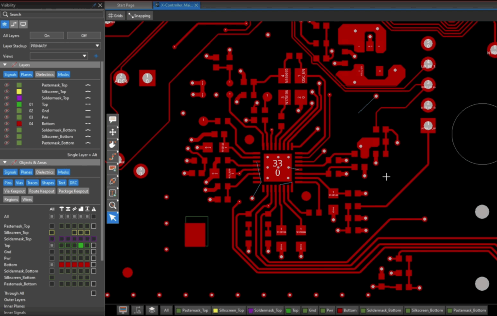
The OrCAD X PCB design software is known for its powerful schematic capture, PCB layout, and advanced simulation capabilities. This software supports high-speed design, including differential pair routing, signal integrity analysis, and constraint-driven design to ensure reliability. The OrCAD X interface is intuitive and features real-time design rule checking and a PSpice simulator for detailed circuit analysis before fabrication. Multi-layer and rigid-flex designs are supported, as well as 3D visualization and seamless integration with manufacturing outputs such as Gerber and IPC-2581. In addition, OrCAD X offers optional cloud-based project management and collaboration tools, making it a preferred choice for PCB engineers.
Altium Designer
PCB design software Altium Designer is known for its integrated and user-friendly environment, which combines schematic capture, PCB layout, and design verification into one tool. Advanced routing features include interactive routing, auto-routing, and high-speed design support, such as differential pair routing and length tuning. Engineers can test designs in a realistic environment and ensure mechanical compatibility with its real-time 3D visualization. Powerful simulation tools for signal integrity and power analysis and a vast component library with live supplier links are included. Professional engineers and teams like Altium Designer because it supports multi-board and rigid-flex design, cloud collaboration, and seamless integration with manufacturing outputs.
PADS
PADS is a professional PCB design software from Siemens that offers powerful tools for schematic capture, PCB layout, and design validation. Among its features are signal integrity analysis, constraint-driven routing, and differential pair routing. Engineers can enhance their productivity with PADS’ intuitive user interface, real-time design rule checking, and advanced autorouting capabilities. The software includes 3D visualization for mechanical integration, thermal analysis, and design-for-manufacturing checks. With robust component library management, simulation tools, and seamless collaboration features, PADS is popular with engineers for PCB design.
Autodesk Eagle
The Autodesk Eagle PCB design software is known for its intuitive interface and powerful schematic capture, PCB layout, and circuit simulation features. It supports multi-layer board design, interactive routing, and advanced design rule checking to ensure high-quality layouts. For seamless collaboration between mechanical and electrical design, Eagle offers an extensive component library, customizable design blocks, and integration with Fusion 360. To optimize PCB designs, the software includes auto-routing, push-and-shove routing, and real-time 3D visualization. Furthermore, its cloud-based project management and version control make it a popular choice for engineers and makers.
DipTrace
A user-friendly PCB design software, DipTrace provides powerful schematic capture, PCB layout, and 3D visualization tools. It supports multi-layer board design, high-speed routing, and differential pair routing. DipTrace includes a hierarchical schematic editor, real-time design rule checking, and an extensive component library with customizable footprints and symbols. A built-in 3D preview ensures mechanical compatibility, while its advanced autorouter and manual routing tools enhance design efficiency. Furthermore, DipTrace supports various manufacturing output formats, including Gerber, DXF, and STEP.
KiCad EDA
KiCAD is open-source PCB design software that provides tools for schematic capture, PCB layout, and 3D visualization. It supports multi-layer boards with advanced routing features, including differential pair routing and length tuning. KiCad’s integrated schematic editor enables hierarchical design, and its PCB editor offers real-time rule checking. There is a powerful footprint editor and an extensive component library, which can be expanded with custom parts. KiCad also includes SPICE-based circuit simulations, interactive push-and-shove routing, and seamless integration with external manufacturing tools, making it a versatile choice for hobbyists and professionals.
EasyEDA
An easy-to-use web-based PCB design software, EasyEDA combines schematic capture, PCB layout, and circuit simulation. Beginners and professionals alike will benefit from its intuitive drag-and-drop interface. EasyEDA provides a comprehensive cloud-based component library, real-time collaboration, and seamless integration with popular PCB manufacturers for quick prototyping and production. Multi-layer designs, interactive routing, and Gerber file generation are all supported. Furthermore, EasyEDA offers SPICE-based circuit simulation, so users can test their circuits before they are built. Since it is browser-based, users can design PCBs from anywhere with an internet connection.
DesignSpark PCB
Free and easy to use, DesignSpark PCB provides schematic capture, PCB layout, and design rule checking. It supports multi-layer boards, manual and auto-routing, and an extensive components library with customizable footprints. The software features an intuitive drag-and-drop interface, real-time design validation, and seamless integration with mechanical CAD tools. With integrated bill of materials (BOM) and pricing tools, DesignSpark PCB is ideal for beginners and professionals. It offers unlimited design space and easy collaboration with suppliers and manufacturers.
The key to maximizing the efficiency of your PCB design workflow is choosing the right software. Choosing the best software for your situation can be a challenge, as there are many EDA tools available. By partnering with the industry leader for delivering software, integration tools and training resources you can mitigate these challenges and arrive at a solution that is tailored to optimizing your design process and board quality.