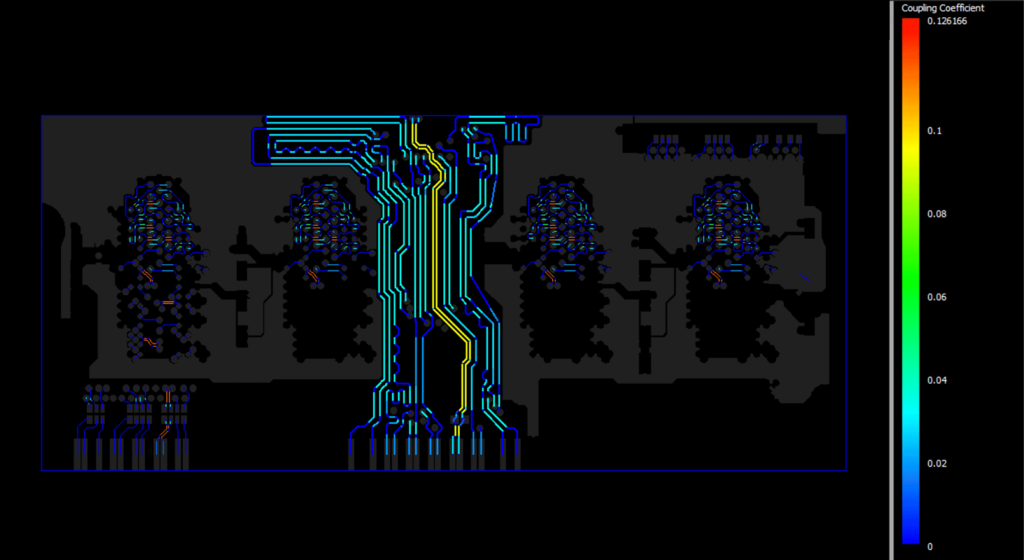
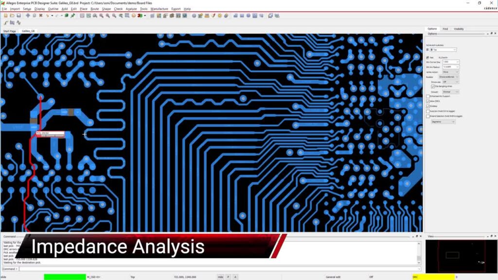
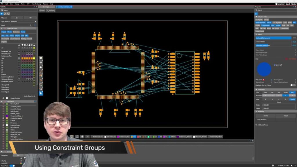
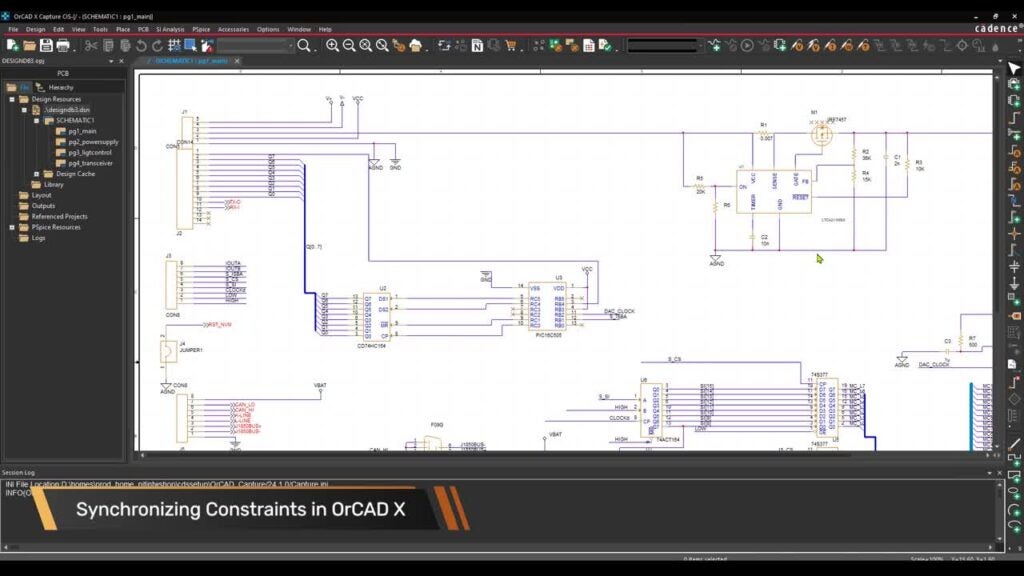
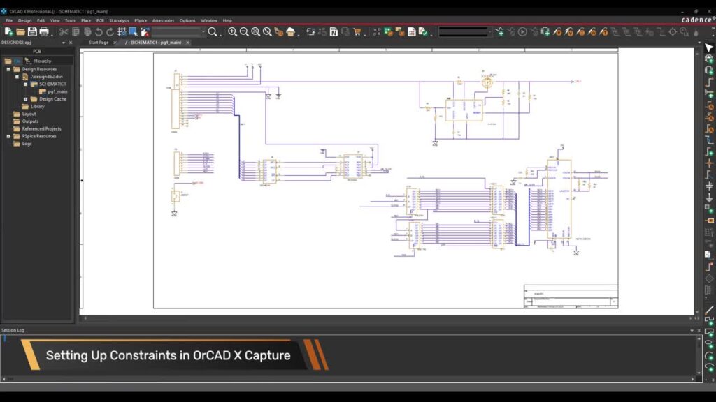
Designing for signal integrity throughout your design will reduce crosstalk, noise and ringing, preserving signal quality and ensuring your design intent. This Whiteboard Wednesday video will discuss how you can consider signal integrity throughout your PCB design process.
Learn more about how the manufacturing process affects the PCB design as well as best practices throughout the PCB design process with our e-book: The Hitchhiker’s Guide to PCB Design.
Be sure to check out some of our other Whiteboard Wednesday Sessions from the PCB Design Experts at EMA Design Automation:
- Team Collaboration
- Best Practices for Component Selection
- Best Practices for Schematic Layout
- Schematic Outputs
- PCB Stackup
- Best Practices for PCB Part Placement: Part 1
- Best Practices for PCB Part Placement: Part 2
- Uses for Copper Planes and Pours
- Via Selection
- Best Practices for Routing
- What is Coupling?
- What is Impedance?
- How to Measure Impedance
- Designing for Signal Integrity
- Designing for In-Circuit Testing
- Designing for testing: JTAG
- Understanding the Manufacturing Process: Part 1
- Understanding the Manufacturing Process: Part 2
- Designing for Manufacturing and Assembly
- PCB Outputs: Fabrication Overview
- PCB Outputs: Fabrication Drawing
- PCB Outputs: Assembly Overview
- PCB Outputs: Assembly Drawing
