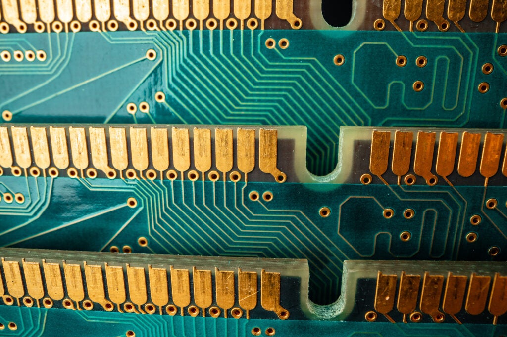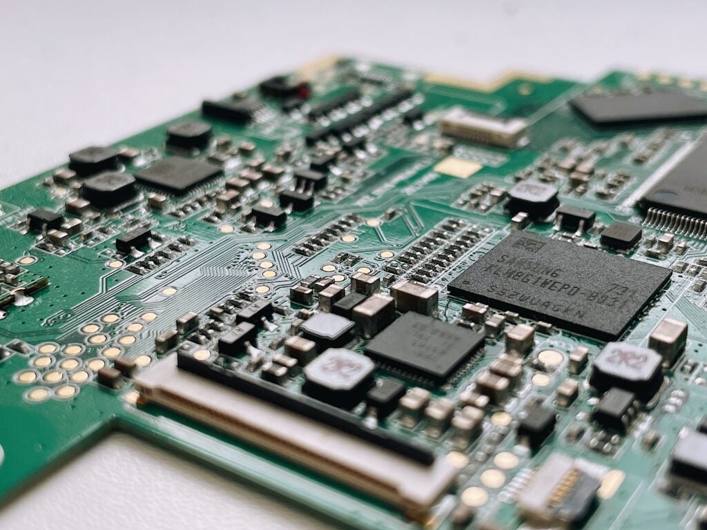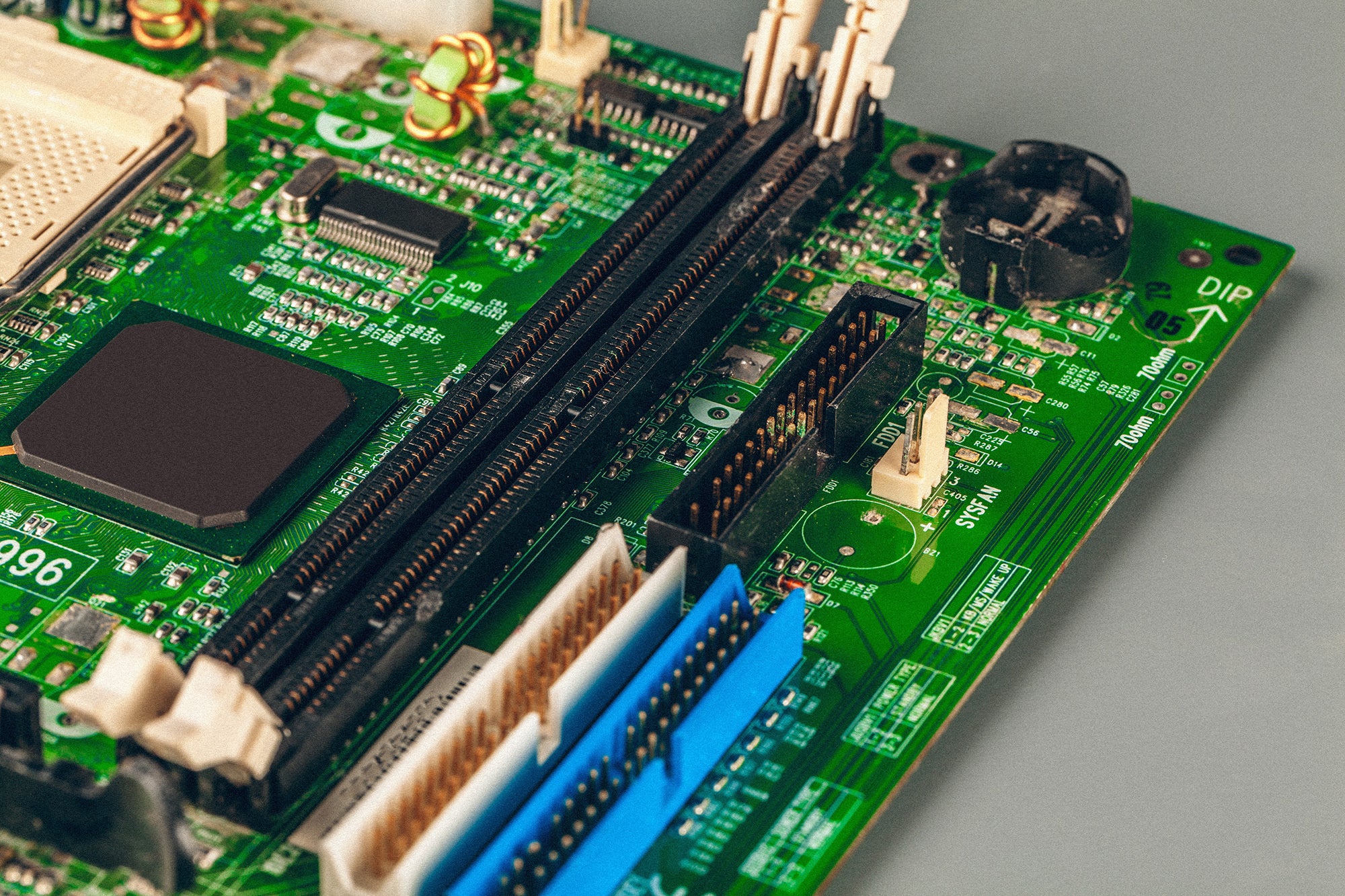
When you’re working on multilayer PCBs, ensuring PCB layer alignment is critical. Even though your EDA software gives you a perfect virtual stack-up, the real challenge emerges during production when every physical layer must be in the right place. Good PCB layer design means that the copper, dielectric, and solder masks all line up as perfectly as possible, ensuring that your board performs flawlessly once assembled. Misaligned layers can lead to connectivity issues, signal loss, and a host of manufacturing headaches, so let’s dive into some best practices that will save you time and trouble.
Why PCB Layer Alignment Matters
Every printed circuit board is built by laminating several layers of copper, prepreg, cores, and solder masks. Although your design software defines the order and orientation, solid PCB layer alignment during fabrication enables the following:
- Reliable Electrical Interconnectivity: Proper alignment ensures your circuit connections are spot‑on and helps you avoid common design for manufacturing and assembly (DFMA) issues that create performance problems; including opens, shorts, or stray couplings.
- Smooth Manufacturability: A well‑thought‑out PCB layer design simplifies circuit board manufacturing steps; such as lamination, solder mask application, and component placement.
- Quick Visual & Automated Inspection: Clear physical markers; such as fiducial marks, let both the human eye and automated systems catch errors early, making it easier to fix issues before they cascade through production.
Properly designed fiducial marks aid in visual inspection and automated PCB layer alignment for assembly
Physical Layer Marking & Orientation
Even if your stack-up looks perfect in your ECAD software, as a designer, you must provide clear physical cues for PCB layer alignment production. Here’s how:
Labeling Each Layer for PCB Layer Alignment
Each layer should carry a physical label. The top layer is marked “TOP” and the bottom layer as “BOT” (in mirrored form). Internal layers should be sequentially numbered in square boxes. This labeling method for PCB layer design makes it easy for all stakeholders to verify that all layers are in the correct order.
Layer Alignment is all about ensuring every layer falls exactly where it should during manufacturing. By clearly labeling and marking the layers, you support both machine-based and visual inspection processes that catch any mis-orientation or registration errors.
How to Label Board Layers for PCB Layer AlignmentIt’s important to follow a universal standard when labeling your board:
|
Stacking Stripes for PCB Layer Alignment
Another smart technique in PCB layer design is using stacking stripes, which are copper markers printed along the board’s edge. For best results:
- Start with a stripe that is 200 mils long and 50 mils wide on the top layer.
- Increase the stripe length by 100 mils on each subsequent layer.
When viewed from the side, these stripes provide an instant visual check that your PCB layer alignment is correct by revealing the sequential order of layers.
Tooling Holes for PCB Layer Alignment
Tooling holes, as described below, are also a great technique for ensuring PCB layer alignment.
- Non-Plated Holes: Incorporate precisely drilled, non-plated holes (usually around 125 mils in diameter) on every layer. Their tight tolerances help “key” the board into alignment fixtures during lamination, solder mask application, electrical testing, and even automated assembly.
- Asymmetric Placement: Using an asymmetrical arrangement (or four holes with deliberate offset) prevents the board from being flipped or rotated, ensuring consistent registration throughout production.
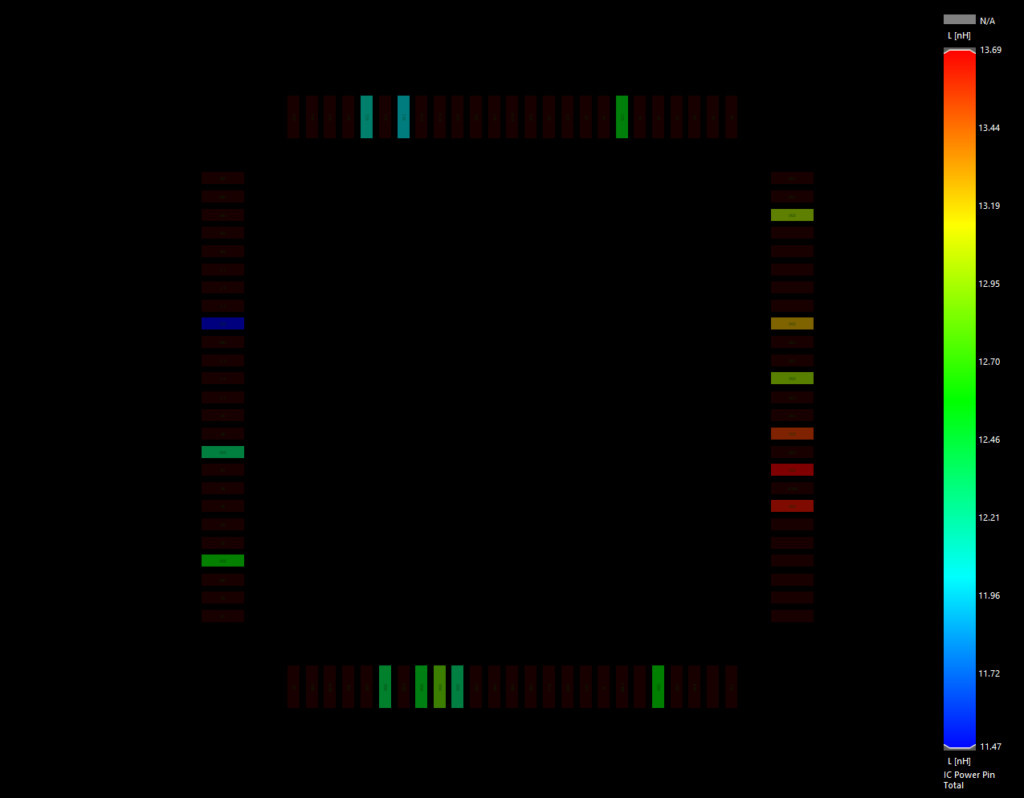
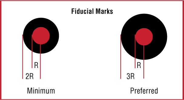
Fiducial Marks
Fiducials are required for machine-based alignment during automated assembly. There are two basic types:
- Global Fiducials are small (about 1 mm) copper dots with a 3‑mm solder mask clearance that act as high‑contrast reference points for pick‑and‑place machines.
- Local Fiducials are placed near fine-pitch areas that help achieve sub‑millimeter component placement accuracy during assembly.
Using fiducials along with tooling holes ensures that your PCB layer alignment remains precise from lamination right through to final assembly.
Best Practices and Considerations in PCB Layer Design
Materials such as copper, prepreg, and solder masks are prone to slight variations (like shrinkage or expansion) during lamination. Do the following to minimize material variations, thus maximizing PCB layer alignment:
- Employ clear and reliable marks on every layer to allow operators to adjust for any deviations.
- Integrate tolerances directly into your PCB layer design features. Always consult with your fabricator to ensure your marks can withstand the manufacturing process.
Maintaining Registration Throughout Production
As your alignment features guide the entire manufacturing process, it is important to follow best practices, as listed below.
- Reuse the Same Registration Features: Use tooling holes and fiducials at every stage—from solder paste printing to component placement and final inspection.
- Panel-Level Alignment: For very small boards (such as those in wearables), alignment features might be built into the assembly panel to maintain precise PCB layer alignment until the boards are separated.
PCB Layer Alignment for Small Boards and Wearables
When designing small boards; including miniature boards used in wearables, PCB layer alignment often requires consideration. Alignment features that may impact your design are described in the table below.