In the PCB design workflow, component placement is the most critical phase. It defines the trace length, the thermal profile, and the overall manufacturability of the board. A common mistake is to view placement as simply “fitting the parts” before the real work of trace routing begins. In reality, a poor placement makes it impossible to complete the routing cleanly, whereas a thoughtful placement often makes the routing straightforward.
Effective placement requires balancing electrical requirements, mechanical constraints, and manufacturing limitations. This guide outlines best practices for PCB component placement to create a clean, functional layout.
Initial Setup and Fixed Constraints
Before moving any individual resistors or capacitors, you must account for the design’s physical realities.
- Mechanical Components: Place connectors, mounting holes, and switches first. These positions are usually determined by the enclosure or user experience requirements.
- Locking Parts: Once fixed components are in place, lock them in OrCAD X or Allegro X to prevent accidental shifts during later stages.
- Board Edge Clearance: Maintain a minimum clearance (typically 50-100 mils) from the board edge to protect traces during depanelization or assembly handling.
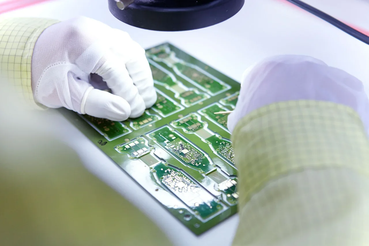
Best Practices for PCB Component Placement
A successful layout follows a logical hierarchy, moving from high-level functional blocks down to discrete passives. Applying the following best practices for PCB component placement will reduce signal integrity issues and manufacturing rework.
Grouping and Logical Flow
The board should reflect the schematic. Components that appear together in the schematic logic, such as a sensor and its local amplifier, should stay together in the layout.
- Partition the Board: Divide the PCB into distinct zones for analog, digital, and power circuitry. This prevents high-frequency digital noise from coupling into sensitive analog signal paths.
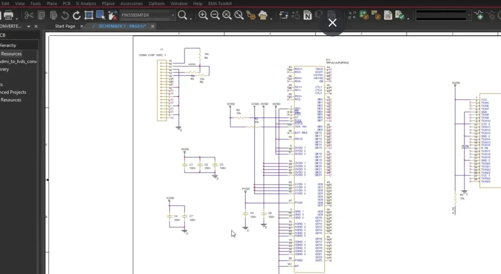
- Utilize Cross-Probing: Use the cross-probe feature between your schematic and OrCAD X Presto. Selecting a group of components in the schematic will highlight them in the layout, allowing you to move entire functional blocks into position at once.
Decoupling Capacitor Placement
Decoupling capacitors act as local energy reservoirs for ICs. If they are placed too far from the pin, the parasitic inductance of the trace renders them ineffective.
- Proximity: Place the smallest-value capacitor (e.g., 0.1µF) closest to the power pin.
- Via Strategy: Keep the path from the capacitor pad to the ground via as short and wide as possible to minimize inductance.
Component Orientation and Spacing
For automated assembly, consistency is vital.
- Uniform Alignment: Try to align similar components (like SOIC packages or 0603 resistors) in the same direction. This improves the efficiency of pick-and-place machines and ensures even heating during reflow soldering.
- Spacing for Assembly: Ensure there is enough room between parts for inspection and rework tools.
Common Component Spacing Guidelines
| Component Type | Min. Spacing (mils) | Reason |
| Discrete Passives (0402/0603) | 10-20 | Prevents solder bridging and allows for rework. |
| SOIC / QFP | 30-40 | Required for visual inspection and pin access. |
| BGA to BGA | 100+ | Allows room for escape routing and X-ray inspection. |
| Board Edge to Component | 50 | Protects parts from mechanical stress during cutting. |
Placement Considerations for Signal Integrity and Thermal Performance
Component placement directly influences both signal integrity and heat dissipation. Poor placement can lead to timing issues, electromagnetic interference (EMI), and localized thermal stress. Below, we address common signal- and thermal-related placement concerns.
Signal Integrity Considerations
Component placement strongly affects signal quality, especially in high-speed designs. Reducing trace length and controlling return paths minimizes timing errors, attenuation, and electromagnetic interference (EMI).
- Place high-speed devices (processors, memory, oscillators) close to the components they interface with.
- Keep clock lines and differential pairs short, direct, and length-matched.
- Maintain continuous reference planes under high-speed signals; avoid routing across plane splits.
- Separate sensitive or low-level signals from high-current or fast-switching circuits to reduce noise coupling.
Thermal Considerations
Thermal performance depends on how heat-generating components are distributed and cooled across the board. Poor placement can create localized hotspots that are difficult to manage and reduce component reliability.
- Distribute high-power components to prevent thermal hotspots.
- Position heat-generating devices where airflow or heatsinking is most effective.
- Avoid placing tall components that obstruct airflow in fan-cooled designs.
- Keep temperature-sensitive components away from major heat sources such as regulators and processors.
Leveraging Cadence Tools for Success
Modern software, such as Cadence OrCAD X and Allegro X, provides real-time feedback to enforce component placement guidelines.
- Design for Assembly (DFA) Rules: You can set specific package-to-package spacing rules in the Constraint Manager. The software will flag a violation immediately if you move a component too close to another.
- 3D Visualization: Use the integrated 3D viewer to check for mechanical interferences. A component might fit its footprint perfectly, but still collide with a daughterboard or an enclosure rib due to its height.
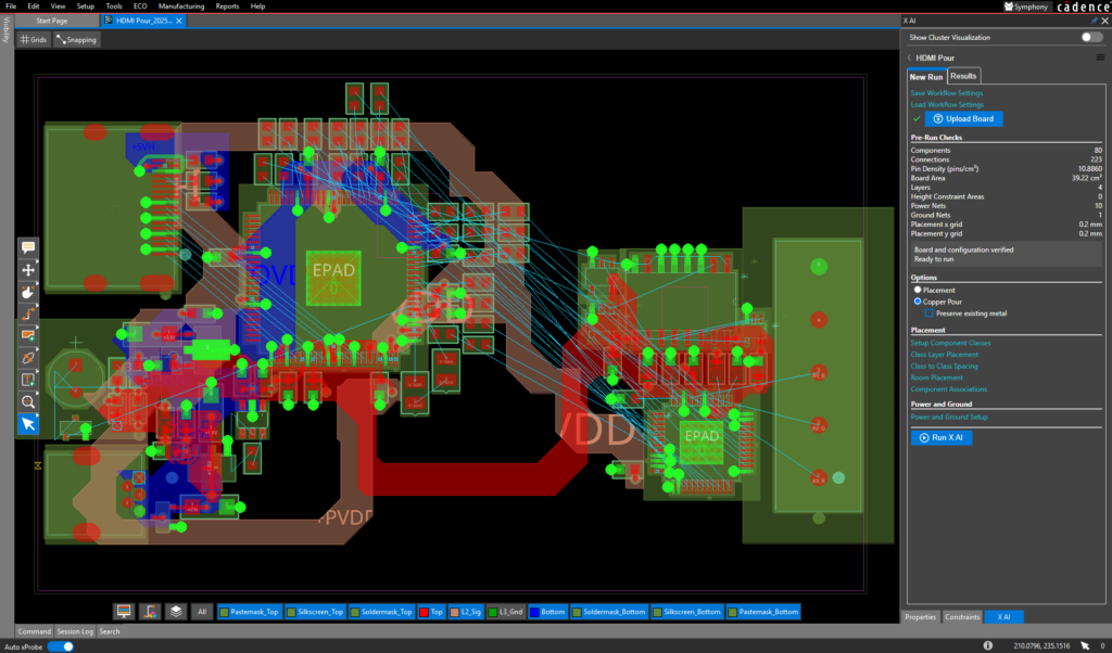
- Flow Planning: For complex designs, use flow planning to visualize the ratsnest. This helps identify where component groups should be moved to shorten bus lengths before you start routing.
Mastering the placement phase is the most effective way to improve your design turnaround time. By applying best practices for PCB component placement, you build a solid foundation for a clean routing process.
EMA Design Automation is a leading provider of the resources that engineers rely on to accelerate innovation. We provide solutions that include PCB design and analysis packages, custom integration software, engineering expertise, and a comprehensive academy of learning and training materials, which enable you to create more efficiently. For more information on the best practices for PCB component placement and how we can help you or your team innovate faster, contact us.