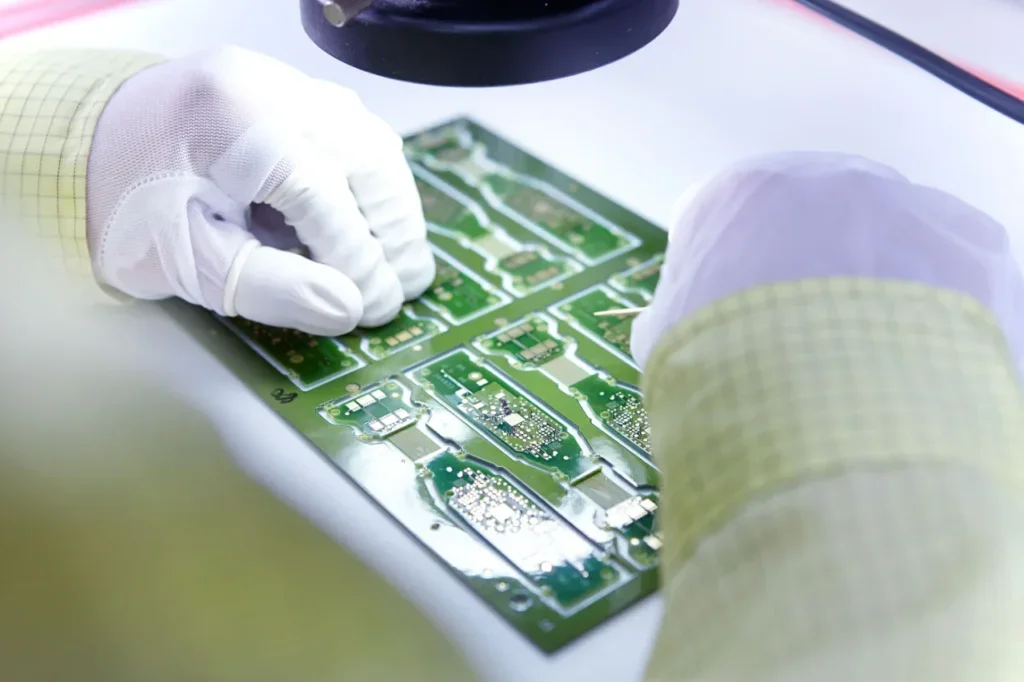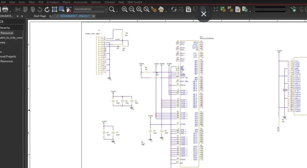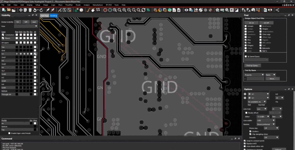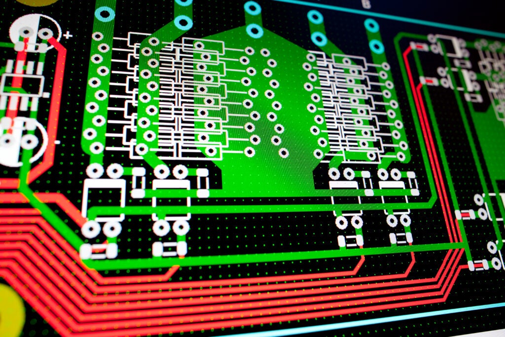
Design reviews are a critical part of the PCB design process. Often a design review consists of a group of people getting together in a conference room to go over a PCB layout. This process can be accelerated or modified to accommodate the new standard of remote working through features such as:
Design review and markup: Highlight sections of the board, embed comments, and tag coworkers to streamline collaboration. Comments are saved within the board file, making it easy to communicate changes and make modifications.
Web-based viewers: Stakeholders can perform design reviews using web-based viewers to eliminate the need to download and maintain the required CAD software. These intelligent viewers provide access to critical design information as well as the ability to comment on the schematic and PCB.
Whether you are an electrical engineer reviewing the layout or a physical design engineer reviewing a coworker’s board (it’s always good to have a second set of eyes), we’ve compiled a list of 6 key issues to catch in your PCB design reviews to avoid costly errors and board spins. These have been determined through years of PCB design services and design reviews performed by our team of experts here at EMA Design Automation.
6 Areas to Check During a PCB Design Review
1. Fiducials
Fiducials are circular or square, solid copper pads which are required to align the PCB during manufacturing to ensure successful assembly. Fiducials have multiple uses during fabrication and assembly including aligning stencils to accurately print solder paste, orienting the pick and place machine, and as an optical reference in Automated Optical Inspection (AOI). During the design review, ensure the board has incorporated both global fiducials and local fiducials.
Global Fiducials: Place global fiducials on the PCB to define the X-Y orientation of the board during manufacturing and assembly.
✅ One fiducial placed in the left corner of the board
✅ 2-3 total fiducials placed in the corners of the board based on the board size
- If the board is large, consider placing additional fiducials in the middle of the board
✅ Do not place global fiducials in a straight line
✅ Fiducials can be placed on the rails of a panel, saving space on the design
Local Fiducials: Place near critical components to ensure proper rotation and placement. This includes:
✅ Fine-pitch components
✅ High pin count ICs
✅ Large BGAs
2. Routing
This critical aspect of the PCB layout defines not only the signal paths but the power and ground distribution networks. Poor routing can lead to a wide range of electrical, thermal, and manufacturability problems and therefore must be a key aspect of the PCB design review. When performing a design review, go above just checking for manufacturability requirements such as trace width and spacing to ensure functionality of your designs by incorporating checks for the following:
Ground Return Vias
Ensure ground return vias are placed near differential pairs when changing layers. When a differential pair changes layers the reference plane also changes. Without a nearby ground via, the return current must take a longer path, which can cause impedance discontinuities, crosstalk, and/or electromagnetic interference (EMI). Ground return vias act as “bridges” for the return currents of differential signals when they change layers, maintaining a continuous, low-impedance reference path and ensuring clean, low-noise transmission.
✅ Incorporate ground vias on differential pairs when transitioning layers
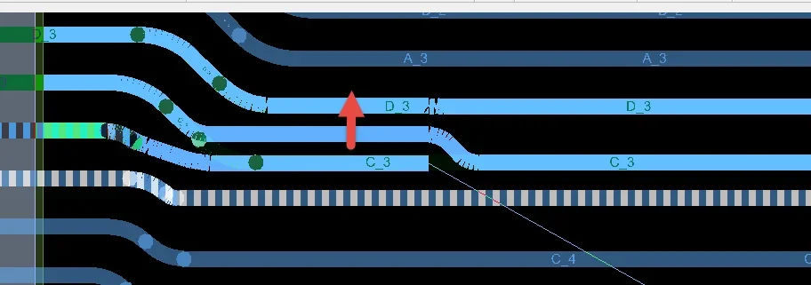
Uncoupled Differential Pair Segments
Verifying the routing of differential pairs and minimize uncoupled trace segments as this will affect differential pair performance. To do this slide traces to ensure nets stay close together when entering/exiting pads and/or when using vias.
✅ Minimize uncoupled trace segments
Routing Distribution
If board space allows, use it wisely. Avoid crowding traces in one area while leaving large unused sections elsewhere. Distribute routing evenly across the board to maintain consistent spacing between traces and nearby components. This approach not only improves manufacturability but also reduces the risk of noise coupling and crosstalk, especially for sensitive or high-speed signal traces.
✅ Space traces evenly
✅ Make use of empty board space
Routing Configruations
Optimize trace routing to maintain short, direct signal paths. Avoid unnecessary bends, excessive length, or sharp turns, as these increase the risk of noise, coupling, crosstalk, and other signal integrity issues. Use trace sliding or automated smoothing tools to streamline routing paths and maintain 45° trace angles to ensure cleaner transitions and improved electrical performance.
✅ Keep traces at 45° angles
✅Avoid unnecessary bends
✅ Keep connections short and direct, unless matching length
Geometry Comparisons
During the PCB review process, it is important to compare similar layouts and geometries across the board to ensure design consistency and identify potential routing anomalies such as stubs, discontinuities, or geometric outliers. These irregularities can disrupt signal integrity, particularly in high-speed or high-frequency designs, where even small deviations in trace length or shape can alter impedance characteristics and timing behavior.
Stubs, in particular, are a common concern as they act as unintended transmission line extensions that can reflect signals or function as antennas, radiating electromagnetic noise to nearby circuits or layers. This can lead to increased EMI, signal distortion, and reduced overall system performance.
✅ Create consistent geometries
✅ Remove stubs
3. Clearances Between Layers
As modern PCB designs grow increasingly dense and complex, ensuring proper electrical spacing is critical not only in the X-Y plane (on the same layer) but also along the Z-axis (between layers). Traditional creepage and clearance checks focus on surface spacing between conductive elements; however, high-voltage, high-density, and multilayer designs demand a more comprehensive approach that includes interlayer separation to prevent electrical arcing, dielectric breakdown, or insulation failure.
To maintain both functional reliability and safety compliance with standards such as IPC-2221 and IEC 60950, designers should verify that sufficient dielectric material exists between copper features on adjacent layers. This becomes especially important in boards with high voltage differentials, thin dielectrics, or tight stackups. When completing the PCB design review:
✅ Perform design rule checks (DRCs) that evaluate creepage and clearance in all three dimensions, not just across the board surface.
✅ Validate dielectric thicknesses in the stackup to ensure adequate separation between conductive layers and adherence to required safety margins.
✅ Account for manufacturing tolerances, as variations in prepreg or core thickness can impact interlayer spacing.
4. PCB Warpage
Maintaining uniform copper distribution on both sides of the PCB core is critical to minimize board warpage during fabrication. PCBs are constructed by laminating multiple cores together, and variations in copper density on each side of the core can create uneven mechanical stresses, leading to bowing or twisting of the finished board.
To ensure successful fabrication, designers must understand the core materials and the differences between prepreg within the core—which is fixed and cannot be adjusted—and prepreg between cores, which can be modified to help balance the structure. Uneven copper distribution may prompt the contract manufacturer to halt production and request adjustments, such as adding thieving patterns or modifying the stackup.
While thieving can be applied to balance copper, an effective alternative is the strategic incorporation of additional ground pours. This approach not only helps achieve more uniform copper distribution, reducing the risk of warpage, but also provides enhanced shielding and improved overall signal integrity.
✅ Review copper distribution on each layer
✅ Incorporate additional ground pours to increase uniformity
5. Acid Traps
Acid traps occur in PCB layouts where acute angles exist between traces or copper shapes. During fabrication, particularly in the etching process, acid removes unwanted copper, and boards are subsequently rinsed to neutralize the chemical. Acute angles can trap residual acid, allowing it to continue etching localized areas. This can lead to over-etching, thinning of traces, or even opens, especially on fine traces (e.g., 4 mils). To mitigate acid traps during the PCB design review process:
✅ Identify and eliminate acute angles between copper shapes and traces by sliding or rerouting traces.
✅Utilize automated design rule checks (DRCs) in PCB layout software to flag potential Design for Manufacturing (DFM) issues during design reviews.
✅ If removing the acute angle is not feasible, add copper fills or shapes to reinforce the connection and eliminate the trap simultaneously.
6. Plating
When designing a Printed Circuit Board (PCB), selecting the correct plating is a critical decision that depends on the product’s classification, end-use, and performance requirements. To determine the correct plating, an industry-standard classification system, developed by IPC (Association Connecting Electronics Industries), is used to define product performance and reliability and serves as a primary guide for plating decisions:
Class 1: General Electronic Products
This category is for basic, everyday consumer products with a short life cycle, where the primary focus is on function rather than durability. Examples of products in this class include toys, calculators, and other inexpensive electronics.
Class 2: Dedicated Service Electronic Products
These products require a longer life cycle and are used where continued performance is desirable but not mission-critical. Some cosmetic imperfections are acceptable as long as they don’t compromise functionality. Examples of products in this class include laptops, telecommunications equipment, and industrial control systems.
Class 3: High-Reliability Electronics
Products in this class must provide high, uninterrupted performance, as failure is not an option. They have the most stringent manufacturing tolerances and are subject to the highest levels of inspection. Examples of products in this class include aerospace, military and medical equipment like pacemakers.
Depending on the class of the PCB, as well as the cost, solderability, conductivity, corrosion resistance, and mechanical requirements, the optimal plating material needs to be selected for the design. Common options include:
- ENIG (Electroless Nickel Immersion Gold) for excellent solderability and cost-effectiveness
- Hard Gold for durable edge connectors needing high wear resistance
- HASL (Hot Air Solder Leveling) as an affordable option for basic soldering
- Immersion Silver or Tin for high-speed signals or cost-sensitive applications with specific limitations
During the design review, ensure the correct plating material is defined in both the cross-section and fabrication notes. While including the plating material in the fabrication notes is required, also incorporating this information in the cross-section will lead to more accurate signal integrity analysis as well as more complete information for the board house.
PCB Design Review Checklist
The following checklist can be used by electrical engineers and PCB designers to perform a thorough design review of common PCB issues:
Setup & Strategy
✅ Color code critical nets on the board, such as assigning brown to ground, to improve design review efficiency
✅Use different stipple patterns to indicate net variations such as a stipple pattern with brown for other grounds like chassis and analog
✅Start by reviewing each layer individually then look at the relationship between layers
✅ Use embedded comments and markup to streamline collaboration
Routing
✅ Ensure ground return vias are incorporated when switching layers for differential pairs
✅ Minimize uncoupled trace segments for differential pairs
✅Smooth traces to keep connections direct
✅ Avoid crowding traces and distribute routing evenly across the board
✅ Use 45° angles for traces
✅ Compare similar layouts and geometries across the board to identify anomalies
✅ Remove stubs or other irregular trace segments that could act as antennas
Safety & Regulation Adherence
✅ Check spacing and clearances in the Z-axis
✅ Perform 3D design rule checks
✅ Verify sufficient dielectric thickness in the stackup to meet safety standards
✅ Check fabrication notes for plating requirements
✅ Verify stackup or cross-section includes plating
Manufacturing & Assembly
✅ Verify a global fiducial is placed on the left corner of the PCB
✅ Place at least 3 global fiducials placed on the board
✅ Place local fiducials placed near critical components
✅ Check for acute angles between traces and shapes which could become acid traps
✅ Verify unified copper distribution on sides of the core material
✅ Incorporate additional ground pours of thieving to balance copper
Need to review the schematic? Get a schematic design review checklist to streamline the schematic review process.
Conclusion: Ensuring PCB Reliability Through Thorough Design Reviews
Performing thorough PCB design reviews is essential to ensure signal integrity, manufacturability, safety, and overall reliability of your boards. By carefully performing a PCB design review, designers can catch errors early, reduce the risk of costly board spins, and improve assembly success.
Modern tools, including embedded markup, web-based viewers, and automated design rule checks (DRCs) available with OrCAD X, make it easier for teams to collaborate efficiently, whether working in the office or remotely. Leveraging these capabilities allows engineers to systematically identify potential issues, validate design decisions, and ensure compliance with safety and performance standards.
Ultimately, integrating a structured design review process and following best practices will save time, reduce manufacturing risks, and produce high-quality, reliable PCBs that meet both functional and regulatory requirements.