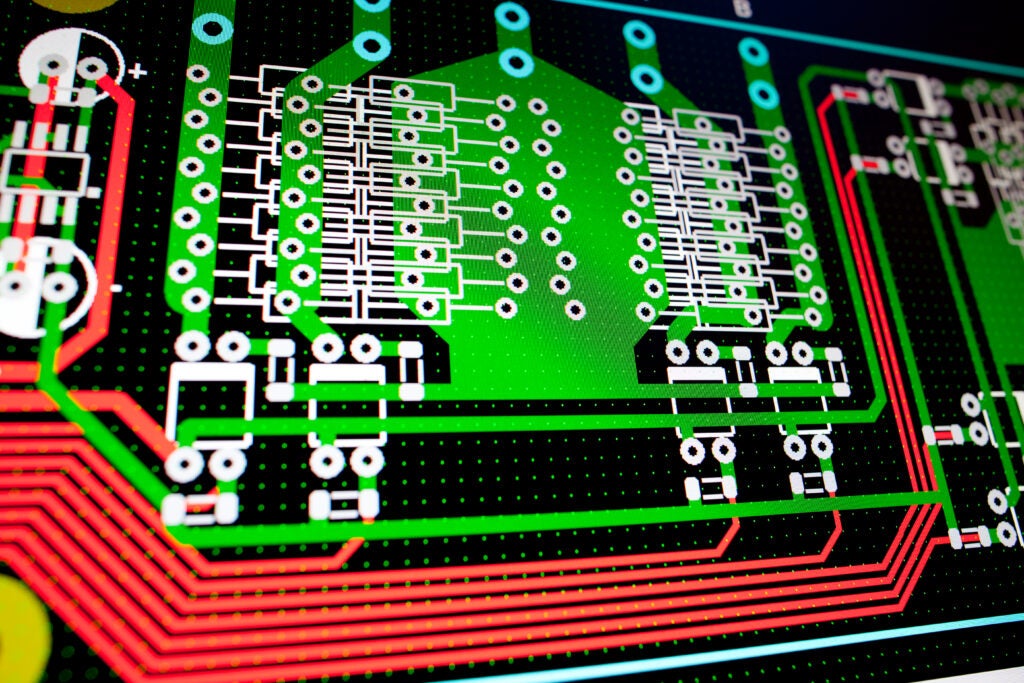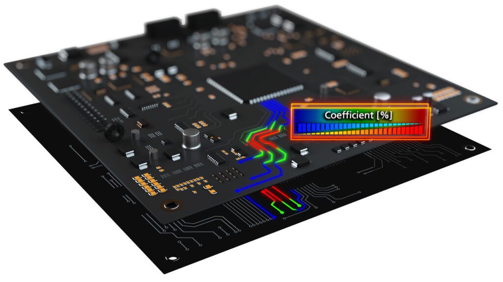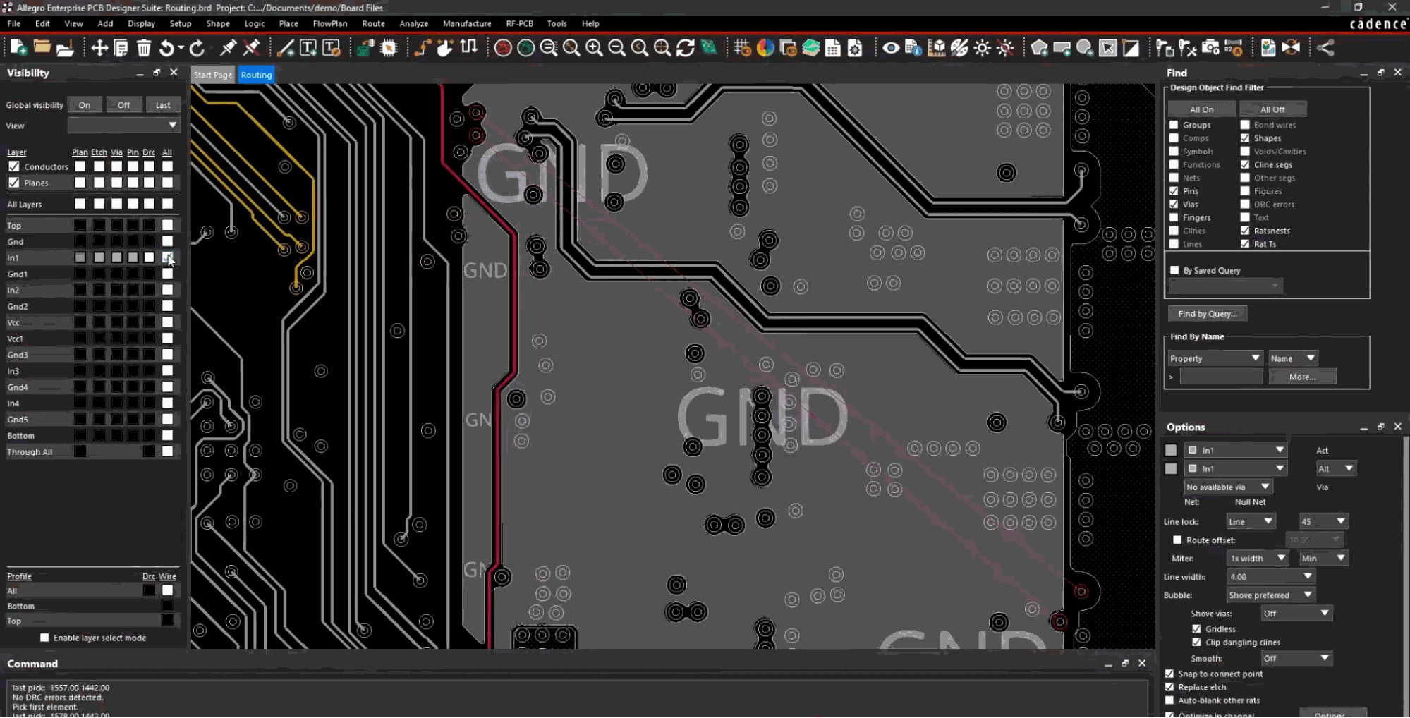
Hug-and-shove routing in Allegro X dynamically moves traces to meet constraints, while shapes automatically adjust without requiring re-pours.
As data rates climb and signal margins shrink, high-speed PCB routing has evolved from a simple connectivity task into a complex engineering challenge. Routing traces for modern interfaces, like DDR5, PCIe Gen5, and 112G Ethernet, require more than just connecting point A to point B. These traces demand a rigorous adherence to signal integrity (SI) principles and manufacturing constraints. For expert designers, mastering Allegro X high-speed routing best practices is key to achieving first-pass success. This guide showcases advanced workflows, from strategic flow planning to leveraging AI-driven automation, ensuring your designs meet the highest performance standards.
Planning for High-Speed Routing
Successful high-speed routing begins long before the first trace is placed. In Allegro X, strategic planning is formalized through flow planning and constraint management.
- Constraint-Driven Design: Do not rely on defaults. Use the Constraint Manager to define rigorous Electrical Constraints (ECSets) for all critical nets. This includes setting up differential pair static and dynamic phase tolerance, maximum propagation delay, and impedance rules.
- Define constraints at the schematic level using logical net classes to ensure intent is preserved throughout the layout process.
- Flow Planning and Bundling: For dense interfaces, such as DDR memory buses or broad data lanes, blindly routing individual nets often leads to the “painted into a corner” situation, where early traces block remaining escape paths. Planning the flow and bundling signals up front prevents these dead ends.
- Allegro X allows you to create bundles of ratsnests where you can define specific routing channels across the board layers, visualizing the flow of data and ensuring adequate space is available between BGAs and connectors.
- Stackup Management: Use the Cross-Section Editor to verify your material stackup. High-speed signals require controlled impedance, which is dictated by the stackup. Ensure your reference planes are adjacent to your high-speed signal layers to provide a low-inductance return path and minimize EMI.
A well-designed PCB is one that is planned in advance and leverages high-speed routing best practices. Here is a list of those best practices for quick reference:
| Allegro X High-Speed Routing Best Practices | |
| Best Practice | Allegro X Feature & Execution |
| Define Constraints Early | Use the Constraint Manager to set rigorous Electrical Constraints (ECSets) for impedance, propagation delay, and phase tolerance before placing a single trace. |
| Flow Planning & Bundling | Create bundles from ratsnests to define routing channels. This guides manual routing and provides the necessary architectural intent for Allegro X AI to generate optimized placements and routing. |
| Phase Tuning & Layer Transitions | Use Phase Tune to correct skew at the source of the mismatch. Always place ground stitching vias next to signal vias during layer transitions to maintain continuous return paths. |
| Real-Time Delay Matching | Activate Timing Vision to overlay color-coded feedback (Green=Pass, Red=Fail) directly on traces. Use Delay Tune to add accordion bumps while monitoring the real-time heads-up display. |
| Assisted Routing Modes | Use Hug Mode to route close to existing copper for impedance control. Use Shove Mode in dense areas to dynamically push traces/vias aside (disable Clearance View during Shove for visual clarity). |
| Route Modifications | Use the Cut Traces (Scalpel) command to slice tuned traces for modification without rerouting the whole net. Use Split Via Stacks in the Slide command to dynamically adjust via layer spans in HDI designs. |
| Return Path & Stub Management | Use integrated analysis to detect traces crossing plane splits (impedance discontinuities). Implement Back Drilling instructions to remove unused via stubs and limit reflections on high-speed nets. |
| Automated Fanout | Utilize Active Route for user-guided, constraint-compliant BGA escape routing and bus routing, leveraging microvias and HDI structures defined in the Padstack Editor. |
High-Speed Routing in Allegro X
Once the strategy is set, execution requires precision. Allegro X offers specific modes and features designed to handle the nuances of high-speed signals. Here are a few Allegro X high-speed routing best practices:
1. Trace Geometry and Routing Paths
Following disciplined geometric practices is the foundation of signal integrity.
- 135° Bends (or Curves): Use 135° bends instead of 90° corners to prevent impedance discontinuities and reflections.
- Direct Routing: Keep critical traces as short and direct as possible. While topology may dictate certain detours, minimizing length reduces delay and loss.
- Daisy-Chain Routing: For multi-drop buses, implement daisy-chain routing rather than long stubs, which behave like antennas and degrade SI and EMC performance.
2. Differential Pair Routing
Differential signaling depends on trace balance and tight coupling. Allegro X provides dedicated tools to maintain this precision.
- Phase Tuning: Use the Phase Tune command to correct skew at its source (e.g., bends or via transitions). Real-time Heads-Up Display (HUD) feedback ensures you remain within spec.
- Spacing Requirements: Maintain consistent pair spacing to preserve differential impedance and keep at least 3× trace width clearance from aggressive signals to avoid crosstalk.
- Return-Path Vias: When changing layers, always place ground stitching vias—or stitching capacitors when changing reference planes—next to signal vias. Allegro X allows you to define via structures that automatically include these return-path elements.
3. High-Density Interconnect (HDI) and BGA Breakout
Dense BGAs and complex stackups require advanced fabrication techniques.
- Microvias and Via-in-Pad: Allegro X supports blind, buried, and stacked microvias defined in the Padstack Editor, enabling efficient breakout and maximizing inner-layer routing channels.
- Active Route: With Active Route, designers can perform user-guided automated routing. The engine follows your sketched path while honoring high-speed constraints, producing clean, manual-quality breakout and bus routing in seconds.
4. Length and Delay Matching
Parallel buses like DDR rely on tightly matched propagation delays. Allegro X streamlines this process through visual guidance.
- Serpentine Routing: When tuning length, keep at least 4× trace width separation between meander segments to avoid self-coupling, and ensure bends are ≥1.5× trace width.
- Timing Vision: Allegro X’s Timing Vision overlays green/red indicators directly on the canvas—instantly highlighting nets that pass or fail timing constraints. Real-time HUD feedback during Delay Tune ensures accurate length and phase adjustments.
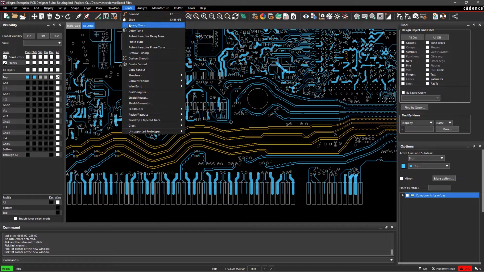
Timing vision helps you easily see real-time delay and phase information right on your canvas.
5. Signal Integrity Visualization and Advanced Mitigation
Allegro X integrates SI analysis to quickly identify and correct physical layout issues.
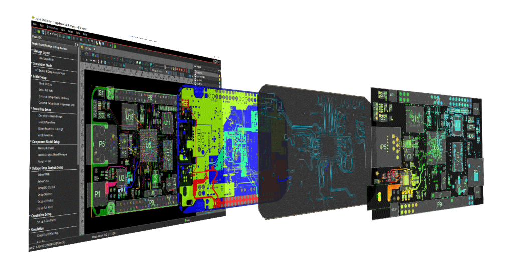
- Impedance and Return-Path Validation: The tool can detect discontinuities caused by plane splits or poor reference transitions. Designers can adjust shapes and immediately re-run checks to verify improvements.
- HDI and Back Drilling for SI: To reduce parasitic inductance and via-stub reflections, Allegro X supports HDI microvias and back drilling, both of which are essential for maintaining impedance on critical high-speed nets.
Assisted Routing In Allegro X
Implementing high-speed traces requires a delicate balance between speed and control. Manual routing can be tedious, while fully automatic routing often lacks the nuance required for strict signal integrity compliance. Allegro X bridges this gap with “Assisted Routing” modes and surgical editing tools designed for high-speed precision.
Assisted Routing Modes
For efficient trace placement, Allegro X offers Hug and Shove modes, allowing designers to route manually while the engine handles real-time DRC:
- Hug Mode: Optimizes board real estate by routing traces as close as possible to existing copper features without violating constraints. Combined with the smoothing engine, it reduces unnecessary vertices to create clean, impedance-controlled paths.
- Shove Mode: Essential for dense designs, this mode automatically pushes existing traces and vias aside to create a valid path.
- Expert Tip: You can enable via shoving in the routing options. However, since Shove Mode dynamically moves copper, it is recommended to disable Clearance View during operation to prevent visual clutter and maintain focus.
- Expert Tip: You can enable via shoving in the routing options. However, since Shove Mode dynamically moves copper, it is recommended to disable Clearance View during operation to prevent visual clutter and maintain focus.
Modifications for Tuned Lines
High-speed designs often require revisions, but modifying a length-tuned, differential pair bus can be destructive if not done carefully. Allegro X provides specific tools for these surgical edits:
- Cut Traces (Scalpel): Located in the Slide command, this tool allows designers to slice through traces while retaining net connectivity. It is ideal for isolating specific sections of a circuit, such as inserting a series resistor or re-optimizing a fanout, without ripping up surrounding tuned lengths.
- Automatic Delay Tune: When combined with Timing Vision, this tool enables quick adjustments to the nets within tolerance.
- Splitting Via Stacks: For HDI designs using stacked microvias, changing layer transitions is often complex. Allegro X simplifies this by enabling via stack splitting directly within the Slide command. By right-clicking a trace connected to a stack, users can select a specific via to split via an intuitive UI. This allows for dynamic changes to layer spans to avoid obstacles or reference plane splits without manual deletion and replacement, with changes previewed in the 3D canvas.
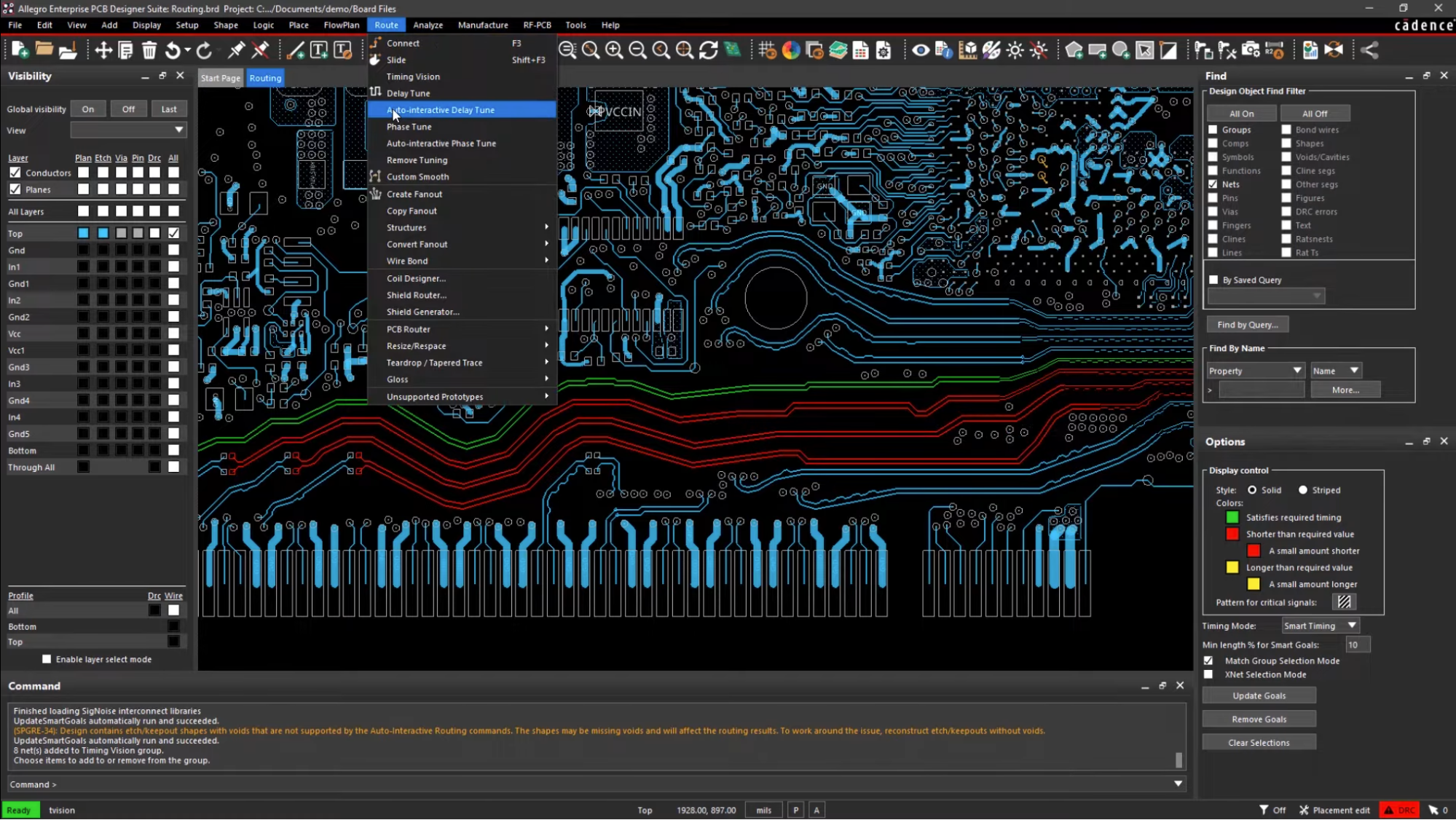
Automatic Delay Tuning quickly brings signals within tolerance
Leveraging AI for Routing Optimization
The sheer complexity of modern constraints can overwhelm even expert designers. This is where Allegro X AI transforms the workflow. By integrating AI, you can automate the most tedious aspects of high-speed routing while maintaining expert-level quality.
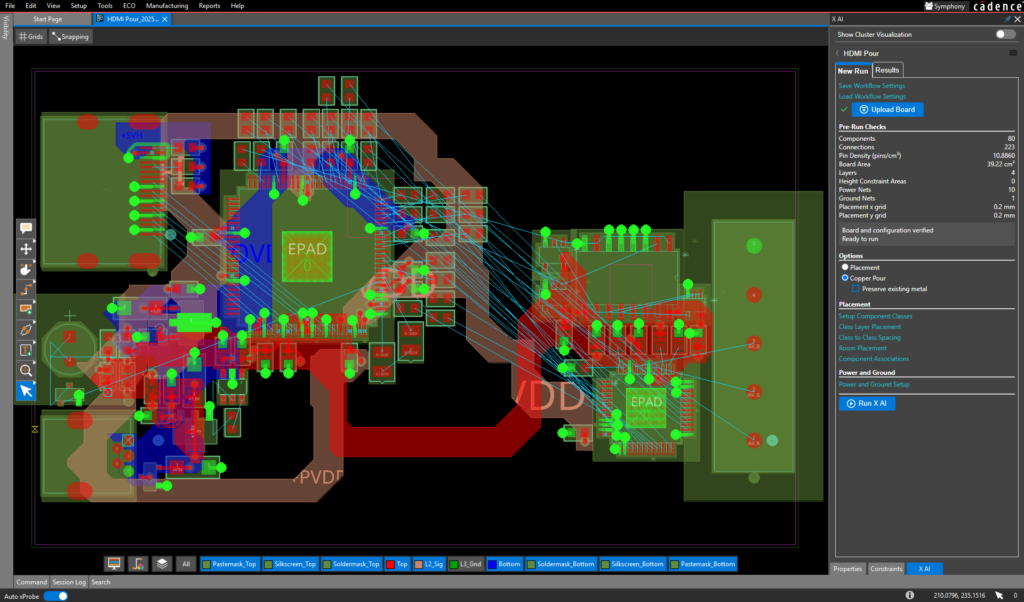
- Automated Flow Planning: Allegro X AI analyzes connectivity and component placement to suggest optimal routing channels, thereby reducing the manual effort required for bundling and planning.
- Smart Tuning: AI algorithms can assist in the repetitive task of delay tuning, automatically adding appropriate serpentine structures to match lengths while respecting spacing rules, freeing you to focus on critical signal path architecture.
- Design-Aware Assist: The AI leverages your existing design data and constraints to make routing suggestions that are context-aware, ensuring that automated edits don’t violate your specific high-speed rules.
- Route AI: Allegro X AI helps determine overall design routability early, allowing you to adjust upfront. Allegro X AI Routing Capabilities are currently available through the Cadence Early Access Program.
Mastering Allegro X high-speed routing best practices involves combining fundamental engineering knowledge with the advanced capabilities of the tool. By using constraint-driven design, strategic flow planning, and the latest AI-assisted features, you can deliver high-performance, manufacturable PCBs more quickly and with greater confidence.
