Feedback regulation loops are widely used by power electronic designers. It is one of the most important and sensitive parts of a power supply circuit. An incorrect feedback loop design may cause oscillations in the circuit, and also increase the output voltage drops. In order to achieve a stable and tight regulation in the output, it is important to have a correct feedback loop.
To test a feedback loop, generally engineers use trial and error methods with the hardware. This takes a lot of time and labor. Moreover, it is expensive because components and/or PCB boards can be damaged. AMS Simulator (also known as PSpice) can be used by designers to test their loop designs without using any physical hardware circuits, and in the process save a lot of time and cost that goes into fine-tuning the design.
To demonstrate a regulation loop and compensator circuit, an example circuit is designed with the MAX8566 component and is available in the Cadence PSpice library.
There are two sections: Open loop design and closed loop design.
Open loop design
You can create an open loop design using the Cadence AMS Simulator (PSpice) tool. Using the component MAX8566 available in the Cadence PSpice library, and the datasheet for MAX8566, you can implement an open loop design as per the following figure:
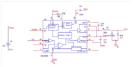
In the open loop design there is no feedback. So the output will increase or decrease with the variation of input voltage. The output voltage is not controlled — hence V(out) increases as the input voltage increases. The goal is to get a constant 1.9 Volts at the output with a variation of input from 2.3 Volts to 3.6 Volts.
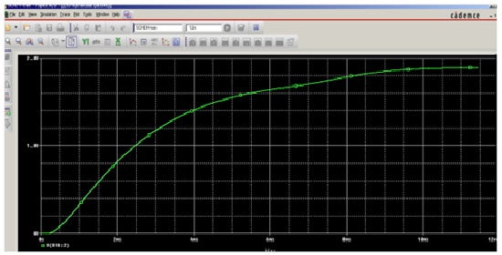
The figure below shows the output voltage waveform when the input supply is at 2.3 Volts, and V(out) = 1.9 Volts
The figure below shows the output voltage waveform when the input supply is at 3.6 Volts, and V(out) = 2.94 Volts
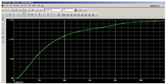
So, the output voltage V(out) increases from 1.9V to 2.94V when the supply voltage increases from 2.3V to 3.6V.
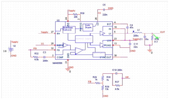
Closed loop design
From the datasheet of MAX8566, Pin 2 is the error amplifier output and Pin 32 is the feedback input.
Pin 25, REFIN, has the reference voltage, which is compared with feedback voltage (FB) to control the pulse width.
From the output filter the corner frequency of the circuit can be calculated as follows:
fcorner=1/(2*Π*√L1*C1)
Since C1 = 33μF, L1 = 200μH, fcorner ~= 2.0 KHz
The filter gives two poles at 2.0 KHz. These two poles produce a phase shift of 180° that makes the output oscillatory. Hence two zeros have to be introduced to cancel the complex poles at the corner frequency and another pole at the origin. This gives a single slope (-20dB/decade) crossing at the ‘0’dB axis, which makes the loop stable. The pole at origin also decides the bandwidth of the converter.
Following the above discussion compensator circuit should have Pole at ω = 0 Hz and Zero at ω = 2 KHz, 2 KHz
Considering all practical conditions, it is advised to choose the Zero location at 1/10th of the calculated value.
For this design, Zeros can be considered at 200Hz. If the transfer function of the following circuit is derived, you can see that there are two zeros at fz1 and fz2 with one pole at fp where
fz1 = 1/(2*Π*R37*C10)= 200Hz
fz2 = 1/(2*Π*R32*C3)=200Hz
fp = 0Hz
After doing all the above changes, the design is ready for closed loop simulation. If simulation is run, following results appear in the PSpice probe window.
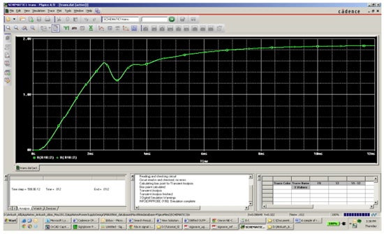
The voltage at OUT is constant V(out) = 1.9 Volt.The user can vary the input supply from 2.3 Volt to 3.6 Volt. The output voltage will be constant at 1.9 Volt. There is no oscillation at output voltage and it is stable.