Fast interfaces and switching speeds are becoming commonplace and with that comes increased noise, amplifying any problems within the power delivery network. Products today are the direct result of the fast signal capabilities in current technology, making it impossible to completely eliminate noise. This noise can be seen in the form of simultaneous switching noise which resonates and can combine to destroy the voltage signal and collapse the signal eye. Therefore, the only viable option is to mitigate the noise via containment.
Managing Switching on Ground
Ground is the point from which we evaluate every measurement, therefore any variation will affect timing and voltage. Every signal switching on the board, whether slow or fast, contributes to noise on the power and ground planes. This “ground bounce” is commonly referred to as Simultaneous Switching Noise (SSN) and is essentially cross talk on the ground.
Since all digital signals share a reference point (in this case ground), if there is too much noise on one section of the board, it can have disastrous effects on unrelated sections of the board. With more ground planes and copper, the effects of SSN tend to be more of a local problem (such as near a chip with poor decoupling capacitors) rather than over the entire plane.
The accumulation of SSN is not easy to visualize in the time domain—multiple signals are turning on and off at certain times and the noise generated from these actions adds up. All the signals on the board are returning through the ground, bouncing their respective voltages. Signals with higher voltage swing can be particularly damaging to faster signals which have reduced margins. These already vulnerable signals, such as timing, memory, or sensors, are the most susceptible to uncontrolled variation on the ground plane. For example, if just one bit of a Data bus is incorrect it can have detrimental effects to the functionality of the design.
Exploring Resonance – Transitioning to the Frequency Domain
While not as intuitive, but equally, if not more important, is analysis in the frequency domain. Utilizing conversion through Fourier transform, we transition from the time domain to the frequency domain. It boils down to basic math, we factor individual complex signals down to its frequency components which are made from sine waves. Signals are then dismantled and factored down into individual waves which can be more easily controlled. Therefore, even though your board may not be operating at a specific frequency, it may still be an area of concern as signals are composed of smaller individual frequencies. When peaks align as we would see with signals of the same frequency, they can add up to sweeping voltage spikes across the board, known as resonance.
Resonance is the accumulation of repetitive small waves that when combined, form a big wave. Think of it as a crowd effect, frequencies with a common denominator and multiples of each other then accumulate. For example, If you’re in a theatre and one person stands up and starts screaming, it’s easy to suppress the noise they’re emitting. However, if there are 5 or more people screaming in that same theatre, it’s a lot harder to control the noise.
It is also crucial to keep in mind that certain regions of the board will echo frequencies better than others. This is directly related to the shape of your copper pour as it can affect resonance by creating a sort of echo chamber on your power plane. Take our theatre example, the size and shape of the theatre itself will also affect how noise is handled: will it be suppressed or amplified?
We can’t approach this as a typical signal integrity problem because all frequencies happen at once—they’re all on the board, at the same time, on the same piece of copper. It’s not an individual effect like reflection or impedance mismatch. We’re dealing with the culmination of multiple signals and frequencies happening at the same time. By dismantling signals into numerous sine waves, we can easily switch our focus and control noise by muting the sine waves with targeted capacitors.
Containment is Key
Luckily, designers have control. Resonance and SSN can be reduced by altering shapes of the power planes or by adding external capacitors. Managing resonance is about balancing the frequencies we inherit due to the nature of the design with what we have control over. If we know signals are made of up sine waves in a specific frequency range, then no matter what the amount of current is, we can control the voltage proportionally by reducing the impedance. The ultimate goal is to have a low impedance over a wide frequency range. To reach this goal, there are three items to keep in mind: copper shapes, the value of any capacitor added, and the way capacitors are attached.
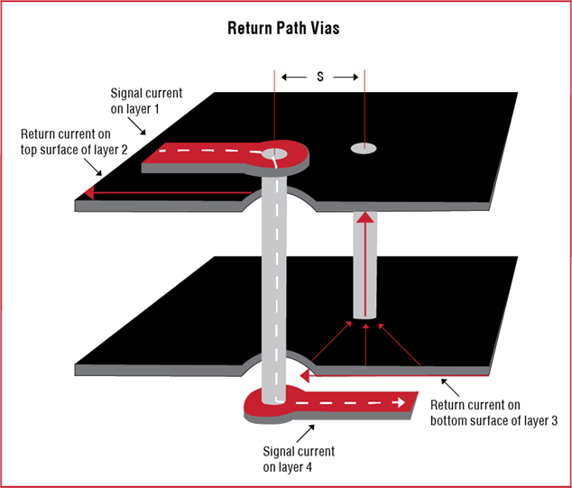
Altering copper shapes can suppress resonance and change the path for the current to flow. Through elongation and notches we can introduce interference, interrupting the echo chamber and steering the signal to where it needs to go. It’s important to steer current away from items such as clocks and oscillators as the noise they create can affect the entire board. This can be accomplished through guard traces, which act as a moat preventing the signals from reaching these critical components.
Modifications on the plane have an effect on the impedance; therefore, It’s imperative to analyze how these changes affect our initial low impedance plan and adjust to meet original goals. Instead of a smooth area for current to flow, the copper is broken up with notches, traces, and vias. This increases the impedance in certain areas of the design. You can suppress areas of high impedance by placing a capacitor to seal the opening at the required frequency.
Resonance can be addressed in a similar way. Placing a capacitor for every frequency on the board is not feasible; however, capacitors targeting certain frequency ranges can combine and reduce the overall impedance. Instead of managing each individual signal, we can eliminate the noise from multiple signals operating in the same frequency range. If we create a smooth enough path by way of low impedance with our capacitors, then there’s no way for that current to generate enough voltage to be problematic.
Cap Selection & Placement Matter
The value of the capacitor and how it is attached have a direct correlation on the effectiveness. To suppress current over a specific frequency range you must identify the ideal capacitor value based on the resonant frequency. This is accomplished by referencing the component datasheet for the optimal performance frequency of the capacitor and matching this up with the frequency we are trying to control on the board.
Once selecting a capacitor to suppress resonance or impedance, we must also control the mounting impedance so the capacitor can be effective. The mounting impedance is made up of the capacitor size, type, placement, routing, vias and the device packaged itself. While this can be done manually, using software and tools can aid in identifying the ideal capacitor value, size, and placement to reduce impedance. Through the process of designing the board, the ideal current flow can be compromised, however through some simple steps, we can contain it.
Power First
If we choose not to address power at the beginning of the design process, we increase the likelihood of discovering catastrophic mistakes late in the design process. The later in the design cycle these defects are found, the more limited our options to resolve them become.
For example, with ground bounce increasing the base of your measurements and resonance decreasing the top margin, it is likely the signal eye will collapse. If this is caught at the end of the design process, there is no workaround that will correct this, the only option would be to change your signal, and even that is not guaranteed to work.
Having a ‘power first’ mentality addresses power issues and influences decisions throughout the design process to prevent this from happening.
Power should not only be addressed first, it should be incorporated throughout your analysis process as well. Power and signal integrity are intertwined as issues within the power delivery network can have a direct effect on your signal quality. Looking at your design as a whole and incorporating signal and power integrity in tandem is the next step. This is where co-simulation comes into play.
Continue reading this series to learn more about incorporating power delivery network analysis into your design process with Jernberg PI #6: Your PDNs Other Job – Closing the Loop with the Return Path.
Contact us for more information on how Sigrity can be used to analyze signal integrity and power integrity for PCB Designers.