We’ve discussed the importance and care required when routing the power delivery network (PDN) of modern printed circuit boards. From how to support current supply needs, loop inductance, to defining layer stack-ups, it may seem like we’ve addressed all the power concerns one could have. However, this is just a fraction of considerations a designer needs to keep in mind. The PDN has an important secondary role which has nothing to do with power delivery. Often forgotten, the PDN is responsible for roughly 50% of the conduction avenues for the non-power signals.
Commonly referred to as return path, this routing “completes the loop”, enabling current to flow. It can be as influential (and problematic) to our signal quality as the transmission lines we study in detail. In fact, failure to address the return path is already a leading cause of signal integrity issues. Perhaps more troubling, they frequently go undetected even in the setting of comprehensive simulation.
The Perfect Plane Promise
Historically, we’ve approached the transmission line (formed each time we connect two IC’s with PCB etch) from a two-dimensional perspective. We typically place and route boards from the top view utilizing the visualization capabilities of our layout software to move up or down the layer stack (the third dimension or Z-axis). It’s common to have power plane layers not visible, frequently unrouted, or even empty until well into the layout timeline. Both PCB layout practice and the simulation techniques that follow it rely on a simple assumption.
Both power and ground will be supplied to each chip, will continue, uninterrupted between them, be added in later, and will be beautiful. So, let’s all just assume “perfect planes”.
For a long time, what reads as sarcasm was in fact true. For the frequencies we were interested in, PCB designers have done a remarkable job in routing boards such that both the power and ground planes have in fact been “electrically perfect”. This is because the many perforations from drill and via anti-pads remained small enough to go electrically unnoticed. So, what has changed? Volumes of studies, articles, and even textbooks have been written to address this very question, but they generally fall into two categories, the planes are much less “continuous,” and the signals are much less forgiving.
Not So Perfect Anymore
Let’s look at the power planes themselves first. High density packaging, fine-pitch devices, and tightly packed vias have combined to reduce the amount of copper that remains when a plane layer is manufactured. Further complicating this, the copper that does remain is often partitioned so several voltages can share a single physical layer, creating additional voids. Complications from this layer sharing can also act to sabotage the “continuous plane” goal as factors like current demand, safety clearances, and filtered power, further influence the chopping of the plane. Known among industry veterans as the “Swiss cheese effect,” it is most noticeable for the power planes, but also effects ground. The same miniaturization effort for which we chop up the power planes has led to layer reduction as well. Typically, as designs have evolved, the ground layers suffer due to the substantial reduction in conducting copper. Collectively, these perforations and separations create at best bottle necks and at worst flat-out obstructions to the very current flow we’ve historically assumed uninterrupted and ignored. (Remember the “perfect plane promise”).
As our planes get less perfect for the reasons above, we must revisit the determination that they can be assumed “electrically perfect” for the purposes of signal integrity simulation. What we find is the signals themselves are also becoming less forgiving of these return path imperfections. It’s the least desirable situation: the returns are becoming less perfect as the signals are becoming more susceptible to the imperfections. Simply put, as our signals get faster (the natural progression of hardware development), smaller interruptions become more significant. This is like how a 30 second stop light becomes more significant on our drive from first street to fifth street, than from first street to Boston . As signals get faster, even if the return path imperfections haven’t gotten worse (they have) their relative size and significance has increased significantly.
Addressing the Return Path Dilemma
The most challenging component of the return path dilemma is “awareness”. Even those convinced to make routing power and ground a priority, often do so with a focus only on power delivery. Many forget the critical “return path” function that same copper is responsible for. No board would be considered for production with a signal routed on two layers, WITHOUT a via or pin to complete the conductive path. Yet, the same type of interruptions in the conductive loop go unquestioned daily when they occur on the return path.
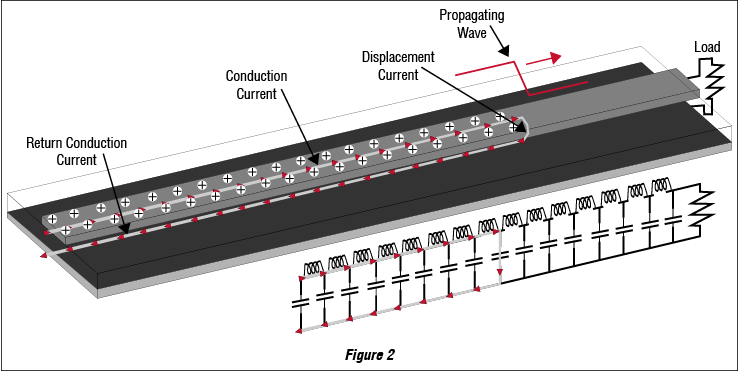
To understand this, we need to review a bit of transmission line physics. As digital data is transmitted from driver to receiver, each transition creates an electrical “edge” which propagates along the transmission lines’ length. It is this edge, and the effects they cause, that we study in Signal Integrity. Traveling with this edge (on the nearest conductor it can find) is the return current energy. The steeper the edge, the more that return path energy stays closely concentrated near it, following it from driver to receiver. Much like the lanes on a highway, signals are transmitted over the routed conductors from source to destination and return on conductors (lanes) in close proximity, often parallel. However, what is not considered is the way energy moves. We mistakenly visualize each bit from traveling source to load and it’s return energy reversing that, running load to source.
Extending our highway analogy, we would be more accurate if each car traveled only a single exit, passing its “energy” to the next in line and returning on the parallel lanes immediately. We would see traffic (current flow) on the home bound lanes well before the message even made it to the destination. Consider the case where somewhere on the path those return bound lanes were interrupted, failed to connect, or were otherwise disrupted, the resulting congestion would quickly impact each exit and ultimately the highway in both directions. This model better represents the energy movement in a transmission, and from it we can make some PCB comparisons.
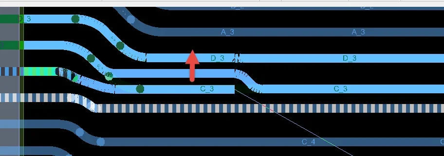
If we are routing a signal trace and it’s first several inches are adjacent to a ground layer, voids in that layer are the electrical equivalent of missing sections of highway. Travelers will eventually make the connection, but may use several inefficient, indirect pathways to do it. Likewise, ground slots, via voids, and plane partitions can cause enough disturbance in the return path conduction to create “issues” as the signal seeks its own path. Frequently these “gaps” in adjacent return copper are easily addressed, but often go unchecked.
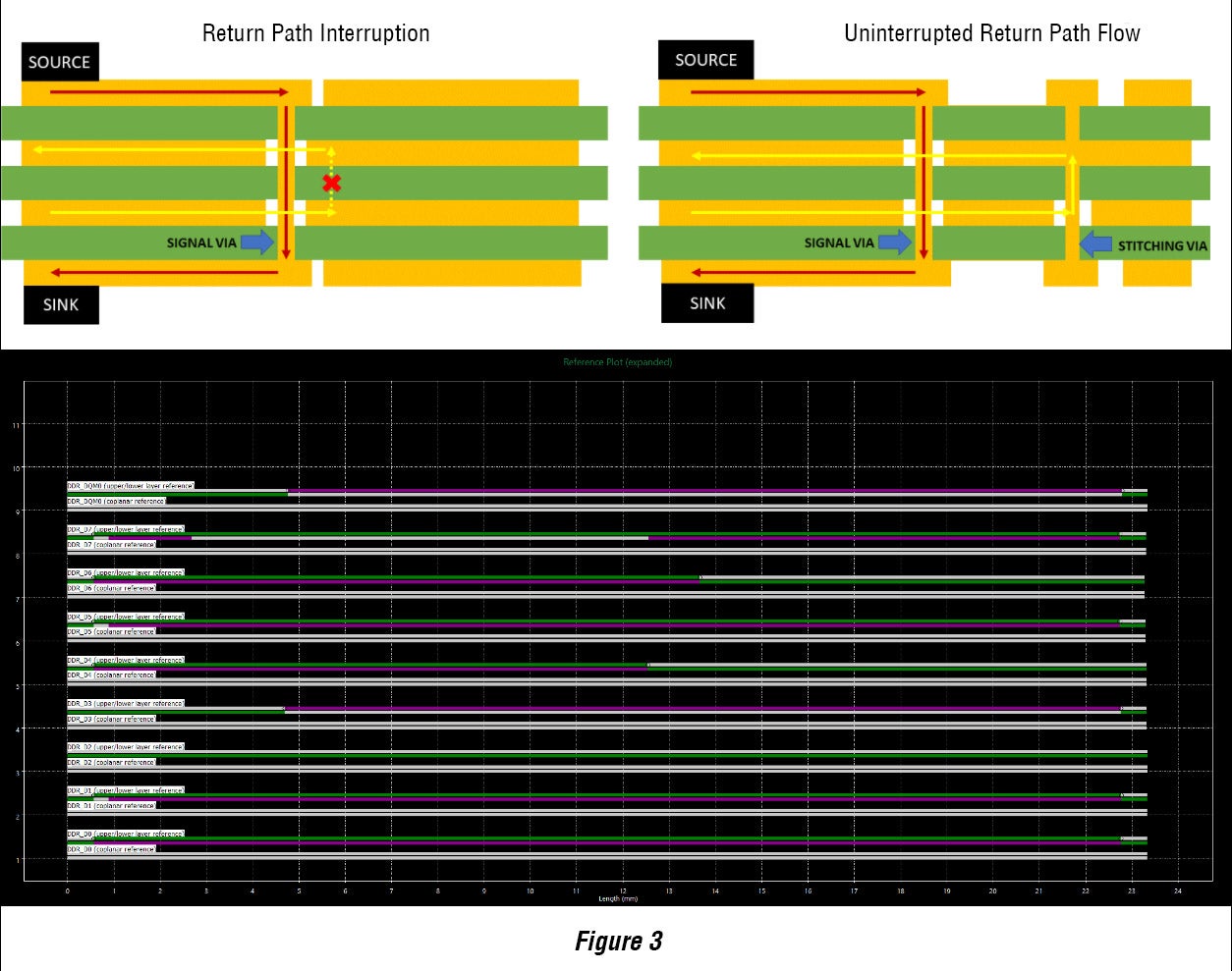
A similar, but even more dangerous situation occurs when the copper on either side of the void is not connected electrically as in the case where a trace is routed over a void separating one power domain from another. The multiple power rails that have become the hallmark of PCB design today almost guarantee these will need watching. Again, the highway can help visualize that. Here we would replace a single section of the return lanes with the lanes of a different highway. Like the original, travelers could use those lane sections in their path, but would need to navigate, getting on, getting off, AND switching from one highway to another. Relating this to our transmission line problem, the concerns are the same. Although there is nothing inherently problematic when a 3-volt signal returns on a 1.8-volt plane, many avoid this condition and several tools are available to identify the “reference changes”. Like the road, so long as the entrance, exit, and plane change have good conductive paths between them there is no issue with the differing levels.
Power is the New Bus
This simple change in the way we visualize the conduction helps us devise a routing methodology that can avoid the most common return path pitfalls. Many are finding success reaching back to methods driven by the wide busses associated with parallel data transmission. Because a bus frequently involves many nets following a similar path to the same chips, they are typically routed (or at least floor planned) first. Recognizing the large swaths of real estate they need, an initial plan or partial route almost always occurs while placement is still in flux. With a single interface now requiring numerous voltages, power is the new bus on nearly every board. To ensure your PDN is sufficient both in delivery and its ability to provide adequate returns, consideration must start early and be a part of the routing process even in placement and fanout. Route power first; use it as a canvas for the remainder of your routing. This as well as the proper tools can help prevent the two things that get us in trouble: reference changes and routing over splits. Avoiding these where we can (and containing them where we can’t) enables us to maintain our claim to “electrically perfect” planes for the frequencies we’re concerned about and enhances our ability to find problems with a board, before we build it.
Continue reading this series to learn more about incorporating power delivery network analysis into your design process with Jernberg PI #7: The Case of the Missing PDN Owner.
Contact us for more information on how Sigrity can be used to analyze signal integrity and power integrity for PCB Designers.