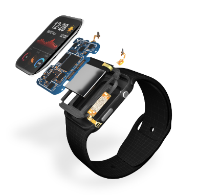
 PCB design is an exciting and fast-paced field in which PCB designers (AKA circuit board designers) implement an engineer’s schematic. While it may sound cookie-cutter, the process is anything but: translating the circuit from an engineer’s schematic to a ready-to-manufacture board file is a cross-discipline exercise that often requires multiple rounds of refinement. This article offers some exploratory steps for those interested in electronic hardware design and wondering how to become a PCB designer.
PCB Designer Complementary Skills
There are multiple options for becoming a PCB designer, as described in the next section. Irrespective of which option(s) you pursue, it is advantageous to have one or more of the following complementary skills.| Complementary Skills for Becoming a PCB Designer EW | |
| Soldering | Gives designers an entry-level skill in manual assembly and introduces them to selecting/working with components. |
| Geometric modeling | Allows designers to gain familiarity with modeling software and the overall design revision process. |
| Bench testing | Assists designers in testing/quality analysis for manufactured boards (especially prototypes during development). |
Options for How to Become a PCB Designer
PCB design falls under the broader discipline of electronics engineering (EE), and a strong background in physics and engineering topics like electromagnetism, materials, and mechanics is beneficial. PCB design was once under the purview of an electrical engineer’s duties, but it’s more accurate to term the work electronic computer-aided design (ECAD). As engineering work has become more demanding and specialized, some organizations leverage designers whose sole role is performing the layout. The PCB designer benefits from knowing the why for layout best practices. However, to avoid future potential issues, design documents should reflect strong engineering principles, yet be understandable to everyone involved in the PCB development workflow. Ultimately, the entire team and the quality of design benefits. If you’re looking to become a PCB designer, consider these options:- Education – While PCB design can be a niche topic through traditional education venues, aspiring designers can find much of the underlying information at community colleges and universities nationwide. Electronics lab work will help build a fundamental understanding of circuit functionality and troubleshoot circuits with diagnostic equipment (multimeter, oscilloscope, etc.).
 Students should focus on courses relevant to the field: electromagnetism and electrical engineering are the clear focuses, but designers will want to supplement these courses by becoming familiar with PCB CAD tools. An introductory robotics course can provide a hand-soldering experience and instruction on component manufacturer part numbers (MPNs).
- Workplace – A less common method for learning the ins and outs of PCB design is starting in a production-floor role with a PCB manufacturer. While there are no guarantees, working “backward” from the shop floor to a workstation is a distinct possibility. This approach gives these designers a leg-up on their peers due to a superior understanding of design for manufacturing (DFM) principles.
- Certification – Many industry and trade associations—for example, IPC and PCEA—offer varying levels of classroom instruction to prepare designers for the rigors of the role. However, these classes can be financially prohibitive for first-time designers or those looking to enter the design field.
- Trade shows – Many trade shows offer designers the opportunity to take courses and network with industry members as they work towards a PCB designer position. Tours of local facilities can also instill knowledge of manufacturing processes and further cement industry relationships. Even more than certification classes, trade shows can be markedly expensive for those looking to make headway as PCB designers. However, some trade shows offer an exhibition day for free meet-and-greet opportunities.
- Online learning – The internet offers ample information for budding PCB designers, including blogs, articles, research journals, podcasts, video workshops, product demonstrations, and more. Open-source layout software also drastically reduces the financial barrier to entry and allows designers to get comfortable with the layout workflow.
EMA Simplifies PCB Designer Workflows
Those wondering how to become a PCB designer may leave this article with more questions than answers – after all, PCB design is a narrow-scope field that can be intimidating to the uninitiated. However, new and aspiring PCB designers can turn to the resources experienced designers use daily in their layout workflows. EMA Academy prepares PCB designers with instructor-led classes, on-demand training, and an expansive how-to library to reduce frustrations and accelerate layouts. With the world-class support of EMA, you can continue to grow your PCB design and ECAD tool usage skills as your career evolves, resulting in improved productivity and performance.EMA Design Automation is a leading provider of the resources that engineers rely on to accelerate innovation. We provide solutions that include PCB design and analysis packages, custom integration software, engineering expertise, and a comprehensive academy of learning and training materials, which enable you to create more efficiently. For more information on how to become a PCB designer and how we can help you or your team innovate faster, contact us.