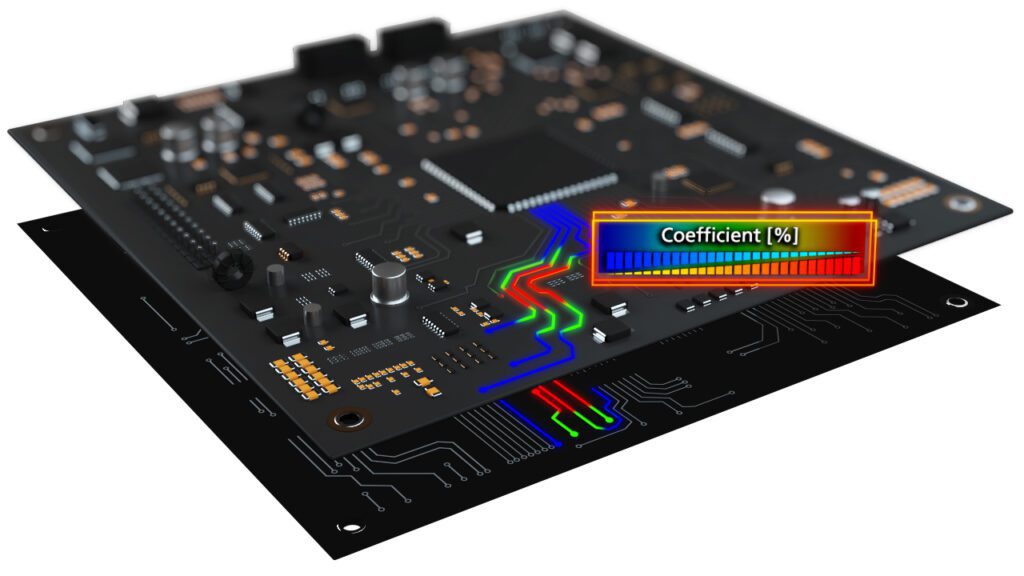
The Power Delivery Network (PDN) is the system of power and ground planes, traces, vias, decoupling capacitors, and any design element responsible for delivering power from the power source to every component on the board. For proper PCB operation, clean and stable power is essential. Components not powering up, intermittent reset or brown-out behavior, noise and instability, and high EMI due to fluctuating power rails are all signs of trouble in the PDN but are hard to identify during testing. Evaluating IR drop as part of the design process can identify common power delivery issues early and ensure reliable power across the board.
What is IR Drop?
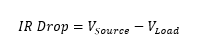
IR Drop refers to the voltage drop that occurs across a conductor due to its resistance when current flows through it. The term “IR” stands for “current times resistance,” representing Ohm’s Law, where:
IR drop can be used to determine the effectiveness of the power delivery network by analyzing the voltage drop as well as the current density across the PCB.
Voltage Drop
Voltage drop is the reduction in voltage or the voltage that is lost as electric current flows through a resistive or impedance path—like a wire, trace, connector, or component.
Current Density
Current density is a measure of how much electric current flows through a specific area of a conductor and identifies areas of concentrated current.
Voltage drop and current density are often analyzed in tandem since they both depend on how current flows through a conductor, and how much resistance that conductor has.
How to Measure IR Drop
IR drop is calculated using Ohm’s law (V=IR) to determine the voltage across the path of resistance and can be measured a variety of ways during the PCB design and testing process:
| Tool | Description | Measurements | Design Stage | Benefit |
|---|---|---|---|---|
| Multimeter | Static measurement between the source and load. | Inexpensive and easy. | ||
| Oscilloscope | Dynamic measurement under load. | Analyzes high-speed behavior. | ||
| Current Probe | Current measurement to be used in IR drop calculations. | Precise dynamic current analysis. | ||
| Thermal Camera | Identifies hotspots from high-resistance PCB features. | Identifies and minimizes overheating. | ||
| Simulation Tools | Simulate and analyzes PDN during the PCB layout. | Pre-layout analysis and optimization. |
Voltage Drop
The first step in measuring voltage drop is identifying the source and load. When testing in the lab, measure IR drop by evaluating the difference between the voltage at the source and the voltage at the load:
In simulations, it is common for the source to be referred to as a Voltage Regulator Module (VRM) and the load to be referred to as a sink.
Acceptable Values for IR Drop
To determine if the voltage drop is acceptable, the following design and component information should be known:
- Required DC operating voltage for components
- Load current or supply current for components
Current values for ICs can be determined from the corresponding device datasheet. Each datasheet will vary for locating the supply current information. Sometimes current values are also listed in the supplier’s page for the IC.
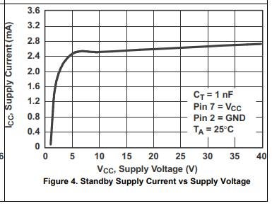
For example, identify the Supply Current vs. Supply Voltage graph. Determine the supply voltage for the design and use the graph to determine the corresponding supply current.
The desired IR drop measurements will vary from circuit to circuit. IR drop is acceptable if the supply voltage at each component remains within its defined tolerance range. If a component’s supply voltage is outside its tolerance range, the component may not receive adequate power, which can lead to undesired operation. At this point, the power delivery network should be analyzed and optimized to improve power integrity.
Current Density
In conjunction to IR drop, current density can be measured to ensure adequate, consistent, and distributed current flow across the PCB. Current density (J) can be calculated through the following equation:
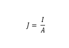
Where:
J = current density (A/mm²)
I = current (A)
A = cross-sectional area of the conductor (mm²)
Acceptable Values for Current Density
As a rule of thumb, if the current-density-to-maximum-current-density ratio is less than 1, the via, trace, and plane design is acceptable. If the current-density-to-maximum-current-density ratio is greater than 1, the via, trace, or plane design fails. In this situation, the power delivery network should be analyzed and optimized to improve current flow.
Measuring both IR drop and current density can help identify insufficient power delivery in your PCB designs.
Common Causes of Insufficient Power Delivery
Insufficient power delivery, measured through IR drop calculations, can arise from various factors throughout the PCB layout. The table below will help to identify the causes of insufficient power delivery, why the PCB feature effects signal and power quality, and a solution to help PCB designers identify and optimize power delivery.
| Cause | Problem | Solution |
|---|---|---|
| High Current Demand | Insufficient power support for sudden or sustained high current draw from components such as FPGAs, CPUs, GPUs, and RF Modules. | Improve decoupling capacitor performance and optimize plane design. |
| Insufficient Copper | Insufficient copper weight or trace widths cannot support the PDN and produce more voltage drop (thin traces have higher resistance and therefore more voltage drop). | Develop a routing strategy and optimize plane design. |
| Poor Decoupling Capacitor Design | Inadequate decoupling capacitor design can lead to instability or voltage ripple. | Improve decoupling capacitor performance. |
| Long Trace Lengths | The longer the trace length the higher the resistance and inductance resulting in more voltage drop especially with high-current designs. | Develop a routing strategy. |
| Via Resistance | Vias introduce resistance and inductance. This is especially problematic in power distribution if many vias are not used in parallel. | Use multiple vias. |
| Improper Plane Design | Fragmented or narrow power and ground planes can bottleneck current and power flow. | Optimize plane design and design for thermal management. |
Understanding the Impacts of Voltage Drop
Voltage drops across a PCB can affect overall system performance and have several negative effects on power quality including the following common power integrity issues:
- Hot Spots
Hot spots are localized areas on the PCB that are significantly warmer than surrounding regions during operation. This thermal concentration can be caused by excessive power dissipation, poor thermal management, or concentrated current density. Hot spots can lead to higher PCB temperatures, potential thermal damage, and reduced battery life.
- Intermittent Failures
Issues within the power delivery network are difficult to identify and troubleshoot, are often inconsistent, and produce failures intermittently.
- Voltage Ripple
Voltage ripple is the small, unwanted variation in the DC output of a power supply. In digital circuits, voltage ripple can cause unstable logic levels, clock jitter, or resets. In analog circuits, voltage ripple produces noise which affects accuracy and performance.
- Malfunctioning or Unstable Components
Insufficient power delivery may result in incorrect component operation if voltage dips below the minimum operating threshold. This can cause unexpected resets, failures, logic errors and corrupted data transmission.
- Increased Timing Errors
Voltage drop can affect the switching speed in digital circuits. Lower voltages produce slower transistor switching and can result in timing violations. This is especially important in high-speed designs which contain critical interfaces like DDR and PCIe.
- Noise
Voltage drops create power supply noise resulting in reduced accuracy, distortion, and instability on power rails which can lead to power supply noise coupling into signal paths.
To prevent these issues, PCB designers must try to create a stable and reliable power delivery network through PDN optimization strategies.
Optimization Strategies for Power Delivery
1. Use Multiple Vias
Multiple vias can be used in parallel to reduce resistance and IR drop and should be added between layers for power and ground connections. Via lengths should be kept short to reduce resistance.
-
-
- Place Multiple Vias in Parallel
- Keep Via Lengths Short
-
2. Optimize Plane Design
Position power and ground planes close to signal layers in the PCB stackup to provide low-resistance paths. When possible, use solid copper planes ensuring power and ground planes are wide and continuous to minimize IR drop, enable stable power delivery, and create a consistent path to ground.
-
-
- Use Solid Ground and Power Planes
- Place Power and Ground Planes Near Signal Layers
-
3. Design for Thermal Management
If the PCB design cannot be adjusted to prevent hot spots and overheating, be sure to design with thermal management in mind. This include using heat sinks, thermal vias, and proper ventilation to manage heat generated by IR drops and concentrated current densities.
-
-
- Use Thermal Vias
- Incorporate Heat Sinks and Ventilation if Needed
-
4. Improve Decoupling Capacitor Performance
Incorporate adequate decoupling capacitors to provide instantaneous power to ICs and critical devices. Place decoupling capacitors as close to the component’s power supply and IC power pins as possible to stabilize voltage and filter noise, reducing the effects of IR drop. Adjust the capacitor size and placement to improve performance and adhere to the IC power demands.
-
-
- Incorporate Decoupling Capacitors
- Adjust Placement and Size to Meet Performance Requirements
-
5. Develop a Routing Strategy
To reduce resistance and in turn the voltage drop across the PCB, keep connections short to minimize trace lengths and increase trace widths. Wider traces have lower resistance, reducing IR drop. Use wider traces for high-current paths.
-
-
- Minimize Trace Lengths
- Increase Trace Widths
-
Incorporating Simulation
To identify where PDN optimization is required in your PCB design, simulation can be deployed to quickly pinpoint IR drop issues, high-current density, and insufficient power delivery. Simulation tools typically calculate and validate IR drop based on the PCB layout and can be used to analyze power integrity and identify IR drop issues created by:
- Insufficient copper pours and traces
- Insufficient via usage
- Long trace lengths
Once these issues are identified, optimization strategies can be incorporated into the PCB design to improve power integrity and the power delivery network.
Why Should You Analyze IR Drop?
Analyzing IR Drop and implementing optimization strategies will improve overall PDN performance by guaranteeing all components receive the required voltage levels without significant drops and achieving a uniform voltage distribution. Performing IR Drop analysis can benefit your PBC design process to:
- Identify Hot Spots
By analyzing the current density of the PCB, you can identify areas with excessive current density that can lead to overheating, reduce reliability, and damage traces. Hot spots can also result in thermal stress and reduce the lifespan of the PCB.
- Reduce Power Starvation
IR Drop analysis helps identify where significant voltage drops occur, which can lead to insufficient power delivery to components. If components do not receive adequate power and the supply voltage falls below the required operating voltage, the component functionality may be compromised.
- Optimize the PCB Layout
Performing IR Drop analysis helps you optimize aspects of the PCB layout to improve power delivery, including:
- Trace Widths: Identify if traces are too narrow to carry the required current without excessive voltage drop.
- Via Count: Identify if there are insufficient vias connecting different layers, which can cause high resistance paths and significant IR drops.
- Component Placement: Determine if critical components are placed in areas where they will receive inadequate voltage, thus affecting their performance and reliability.
- Enhance Reliability
Ensure the PCB operates reliably under various conditions and delivers proper voltage levels to all components.
- Reduce Troubleshooting Time
Power delivery issues are often intermittent, making it difficult and time-consuming to pinpoint issues in the lab. Analyzing IR drop within the PCB canvas allows you to quickly identify and resolve hard-to-find issues and decreases the time spent troubleshooting.
Performing IR Drop analysis at any stage of the design is going to yield benefits but having this as the last step in your design process can result in late-stage design changes, additional rework, and more design hours if any issues are found. Analyzing IR Drop throughout the PCB layout will allow you optimize your PDN design and ensure adequate and reliable power delivery- this is where Sigrity Aurora can help.
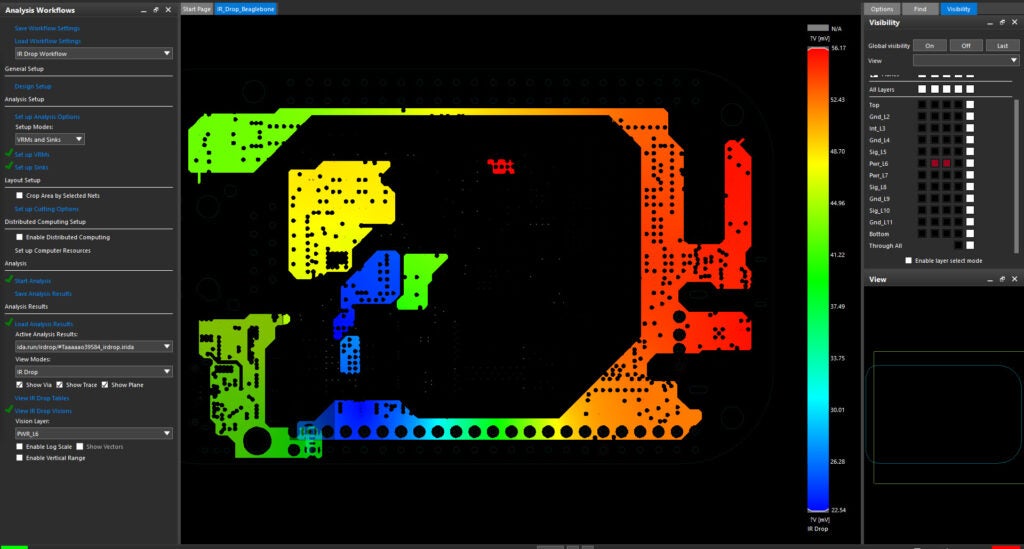
Analyzing IR Drop with Sigrity
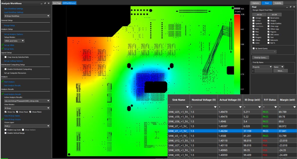
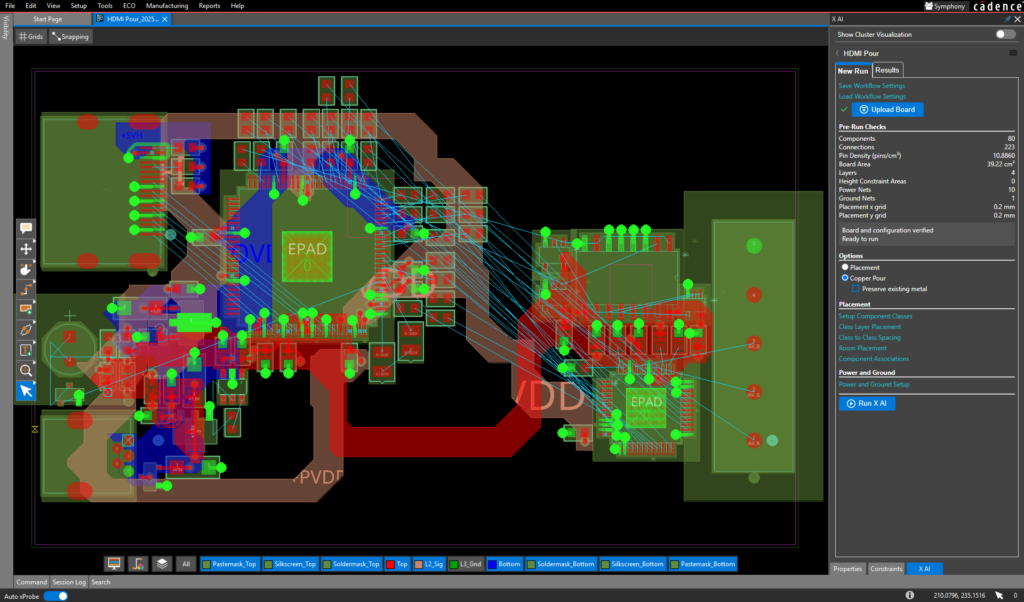
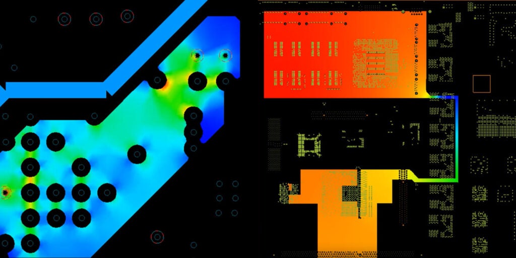
Sigrity Aurora includes easy-to-use workflows that step you through the required procedure to analyze signal and power integrity in your PCB designs. The IR Drop Workflow in Sigrity Aurora is most commonly used to analyze voltage drops and current density, providing a step-by-step procedure to perform layout-based IR drop analysis directly within the PCB layout canvas. The IR Drop workflow can be used by PCB designers throughout the PCB layout process to identify and correct issue when change is easiest, reducing time spent on prototyping, troubleshooting, and redesigning the PCB. Sigrity Aurora streamlines the product development process and allows you to efficiently analyze IR drop with:
- A unified environment for PCB design and power integrity analysis
- Easy-to-use workflows
- Minimal setup and modeling
- Visual overlays directly on the PCB canvas with color-coded results
- Detailed, tabular results to easily pinpoint excessive IR drop and current density
- Easy-to-understand pass/fail results
Learn more about IR drop and how to resolve common power integrity issues using Sigrity Aurora with our free course: Introduction to In-Design SI/PI analysis with Sigrity Aurora.