With the advancements in electronic design automation (EDA), it may be tempting to simply rely on the software for schematic design. Yes, these tools can significantly improve your design process. However, to choose and use EDA software most effectively requires that you know and follow good electronic schematic design guidelines.
Essential Electronic Schematic Design Guidelines
The basic procedures of the two PCB design stages, schematic capture and PCB layout, are well-known. Although these stages are typically performed separately and sequentially, they are not exclusive. In fact, PCB layout efficiency is directly proportional to how well you execute the steps of a good PCB schematic design checklist. This is easily seen by delving into the electronic schematic design guidelines, as listed below, from which this checklist is derived.
| ESSENTIAL ELECTRONIC SCHEMATIC DESIGN GUIDELINES | |
| Guideline | Impact |
| Define and quantify performance goals and constraints | Provides a foundation and metrics on which to base design decisions. |
| Draw a functional block diagram | Simplifies routing and troubleshooting. |
| Choose parts based on verifiable data and information | Ensures performance objectives are met. |
| Verify CAD model accuracy for all parts | Avoids manufacturing issues. |
| Arrange symbols on the schematic as if laying out the board | Minimizes time needed for placement and routing during layout. |
| Run nets based on component pinouts/datasheets | Helps minimize errors. |
| Run design rule checks often | Reduces complexity of error correction. |
| Run functionality and performance simulations during schematic capture | Increases development cost-effectiveness. |
| Create and verify accuracy of BOM | Helps avoid supply chain issues. |
| Run final connectivity verification and fix any errors before starting PCB layout | Minimizes downstream errors that may not be detected before board build. |
As the list above shows, many of the guidelines for your schematic design impact the efficiency of the PCB layout stage. Collectively; however, these guidelines significantly affect the entire circuit board development cycle. And effective implementation is a foundational requirement for PCBA development optimization.
Maximizing Schematic Design Effectiveness
Absent the effective implementation of electronic schematic design guidelines, the complexities of circuit board development can lead to excessive development time before an acceptable high-quality production-ready PCBA is achieved. Therefore, understanding how to best incorporate and follow each of these guidelines, as discussed below, is extremely important.
Define and quantify performance goals and constraints
Clearly defining objectives is the tried and true first step of the scientific method. In most cases, a qualitative goal must be converted into metrics that can be measured and analyzed to satisfy this mandate. This means specifying electrical values–or ranges of values; such as target voltage, current, power, frequency, etc., for inputs and outputs that can be easily checked for compliance.
Draw a functional block diagram
Creating a graphical representation allows you and all other design team members to clearly see all connection points and nets. Not only does this simplify routing, but also makes tracing down root causes of performance errors as straightforward as possible.
Choose parts based on verifiable data and information
To ensure that the parts you choose are able to meet the electrical objectives defined, it is critical that the performance criteria you based your selections on are accurate. Therefore, the reliability of the data and information from your component library resource is imperative.
Verify CAD model accuracy for all parts
The ultimate authority for schematic symbol pinouts, footprints, and landing patterns is the manufacturer. Therefore, CAD models should be directly from the manufacturer datasheet or a component library resource that ensures models are manufacturer-vetted.
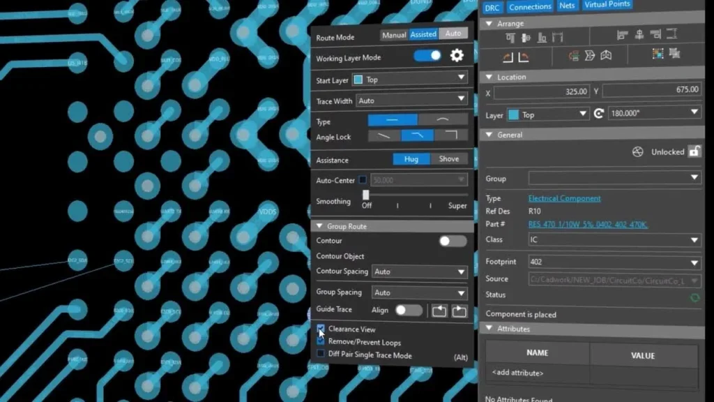
Arrange symbols on the schematic as if laying out the board
PCBA design software programs include automatic component placement. Typically, initial board layout and routing is taken from the schematic. Therefore, significant design time can be saved by placing parts and traces in desired locations during schematic design.
Run nets based on component pinouts/datasheets
Datasheets are invaluable resources for efficient board design. One of the most important to follow are the pinouts that define which pin connections are mandatory and which are optional. Doing so can greatly reduce connection errors.
Run design rule checks often
The question is not whether there will be design errors to be corrected, but how difficult are they to identify and fix. Effectiveness in this endeavor greatly depends upon how well you incorporate and organize the rules of your design program’s online design rule checker (DRC). Failing to prioritize rules correctly can cause severe problems. For example, operational and performance issues; such as floating pins, that go overlooked during design, only to be discovered after board build may require costly redesigns and respins.
Run functionality and performance simulations during schematic capture
For many designs, simulation is critical to verify functionality and performance. SPICE simulation as well as RF simulation and analysis should be incorporated during the schematic phase of design, as needed. Failing to institute and execute these evaluations during design can result in wasted development time, excessive manufacturing costs, and lower profitability and ROI.
Create and verify accuracy of BOM
For PCBA design, building the bill of materials (BOM) is often relegated to an afterthought of the board design process. However, the issues that an inaccurate parts listing can cause are quite significant. For example, MPNs that don’t match footprints can delay manufacturing and increase cost. Even more severe is failing to check and verify component availability, which may result in the need for redesign, as well as, additional manufacturing delays and increased costs. Integrating real-time information from distributors and analyzing supply chain data directly in the schematic can ensure an accurate and purchasable BOM.
Run final connectivity verification and fix any errors before starting PCB layout
Prior to moving a schematic design to PCB layout, a final verification of connectivity accuracy must be performed. Failing to do so, may result in errors that are not discovered until after manufacturing that must be corrected.
Effectively Using EDA Tools to Optimize PCB Schematic Design
Understanding and following electronic schematic guidelines as discussed above provide you with the roadmap for achieving a maximally effective schematic design process. For execution; however, you need PCBA design and development software solutions with the requisite functions and capabilities to satisfy the requirements of the guideline implementation. The best option may be to partner with an experienced provider of EDA tools with a track record of successfully helping engineers and designers optimize their PCBA development processes.
EMA Design Automation is a leading provider of the resources that engineers rely on to accelerate innovation. We provide solutions that include PCB design and analysis packages, custom integration software, engineering expertise, and a comprehensive academy of learning and training materials, which enable you to create more efficiently. For more information on how to best implement essential electronic schematic design guidelines and how we can help you or your team innovate faster, contact us.