Modeling designs helps engineers verify whether their circuit will function as intended. Modeling programs simulate circuit behavior under different conditions and in accordance with the design requirements, allowing engineers to better plan and build circuits.
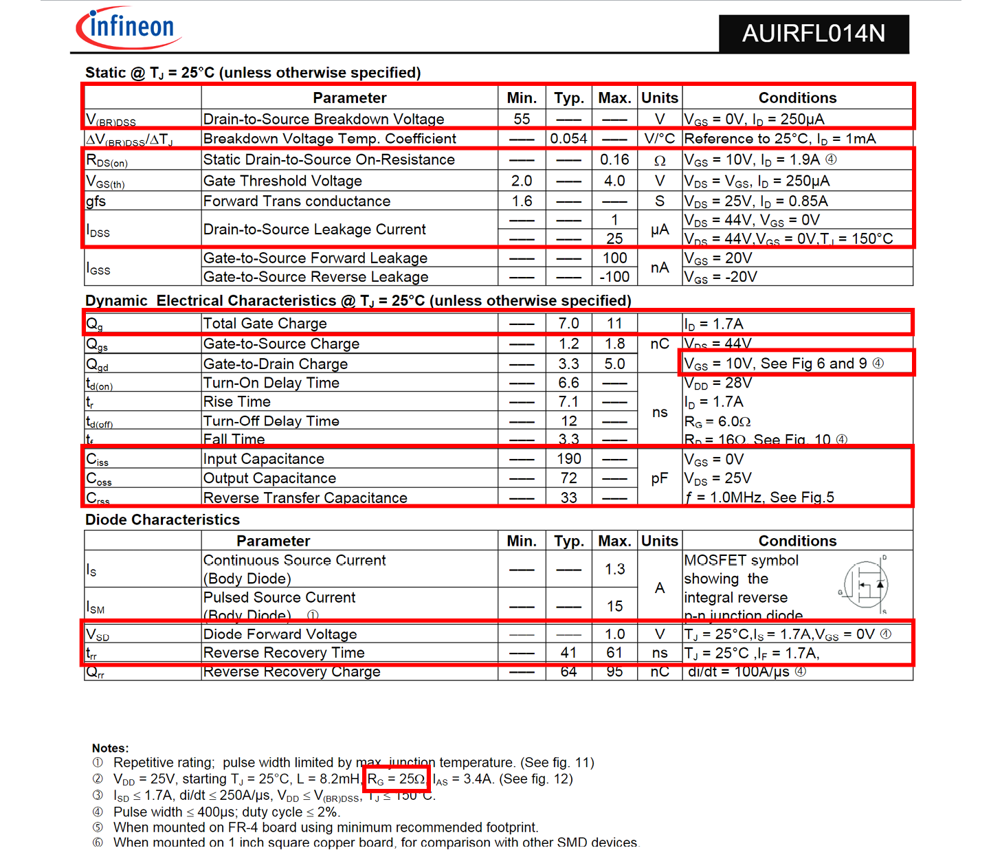
Typically, to model components, generic models are used, which produce inaccurate and unrealistic simulations based on ideal conditions. This can cause functionality issues to go undetected until far later in the design process. To confidently simulate a component, create a Power MOSFET SPICE model using specifications from a manufacturer’s datasheet.
What is a Power MOSFET?
A Power Metal Oxide Semiconductor Field Effect Transistor (MOSFET) is a voltage-controlled device used to switch large amounts of current. Power MOSFETs are frequently used due to their low-gate drive power and fast switching speeds.
What is Needed to Model a Power MOSFET?
To create the required Power MOSFET for simulation, two items must be defined:
- Type
- What type of MOSFET is required: N-Channel or P-Channel?
- Power MOSFET Characteristics
- What are the required parameters for the Power MOSFET: input/output capacitance, diode forward voltage, total gate charge, etc.?
This information must be incorporated into the SPICE simulation model which can be achieved by manually creating or editing a text file. Keep in mind if the model created does not produce the intended outcome or if a part is changed, values will need to be edited manually. This manual process to produce the desired model is time consuming and increases the likelihood of errors; however, the PSpice Modeling App provides a fast, easily-configurable, and fully-integrated method to create a Power MOSFET SPICE Model for simulation.
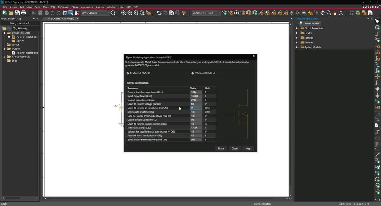
Creating a Power MOSFET SPICE Model with PSpice
The Power MOSFET modeling application quickly creates Power MOSFET models with a wizard-based approach. The parameterized MOSFET enables simulation and testing of the model in various conditions. The necessary specifications are predefined and users can easily input the Power MOSFET characteristics, defined by manufacturers, directly into the parameters:
- Type:
Select either N-Channel or P-Channel.
- Reverse Transfer Capacitance:
Define the small-signal reverse transfer capacitance (Crss). This value must be between 0nF and 10nF for both N-Channel and P-Channel MOSFETs.
- Input Capacitance:
Define the small-signal input capacitance when the drain and source terminals are shorted (Ciss). This value must be between 0nF and 10nF for both N-Channel and P-Channel MOSFETs.
- Output Capacitance:
Define the small-signal output capacitance when the gate and source terminals are shorted (Coss). This value must be between 0nF and 10nF for both N-Channel and P-Channel MOSFETs.
- Drain-to-Source Voltage:
Define the maximum drain-to-source voltage the device can sustain when in the off state (BVDss). This value must be between 1V and 1kV for N-Channel MOSFETS or between -1V and -1kV for P-Channel MOSFETs.
- Drain-to-Source On-Resistance:
Define the electrical resistance when the device is in the on-state. The drain-to-source on-resistance (RdsON) value must be between 1n ohms and 100 ohms for both N-Channel and P-Channel MOSFETs.
- Series Gate Resistance:
Define the Series Gate Resistance (Rg). The gate resistance is caused by the resistance of the gate conductors as well as the metal and contact structures that route the gate signal to the pad for external package connection. This value must be between 1n ohms and 100 ohms for both N-Channel and P-Channel MOSFETs.
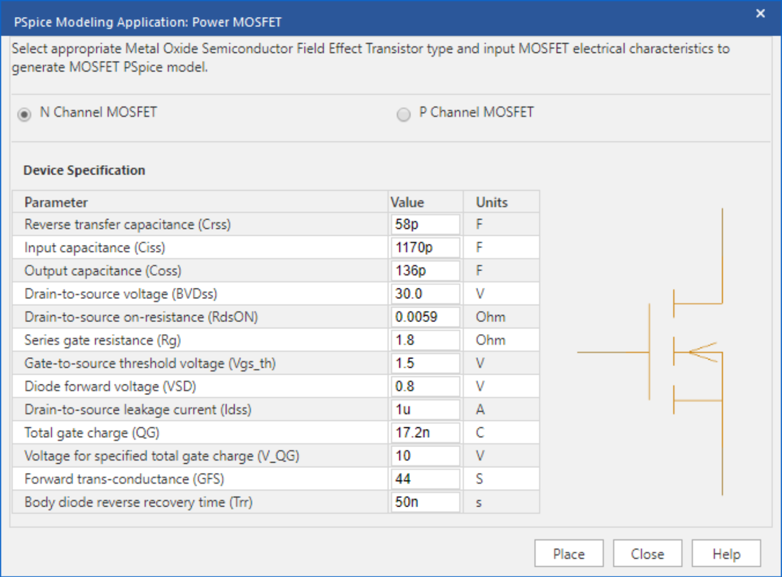
- Gate-to-Source Threshold Voltage:
Define the minimum gate bias which can form a conducting channel between the source and drain. The gate-to-source threshold voltage (Vgs_th) value must be between 1nV and 10V for N-Channel MOSFETs or -1nV and -10V for P-Channel MOSFETs.
- Diode Forward Voltage:
Define the forward voltage drop of the integral body diode when a set current is applied to the source. The diode forward voltage (VSD) value must be between .3V and 1V for N-Channel MOSFETs or -.3nV and -1V for P-Channel MOSFETs.
- Drain-to-Source Leakage Current:
Define the leakage current flowing between the source and the drain. The drain-to-source leakage current (Idss) value must be between 1pA and 1mA for both N-Channel and P-Channel MOSFETs.
- Total Gate Charge:
Define the amount of charge required for the gate driver to turn the device on or off itself. The total gate charge (QG) value must be between 1pC and 100uC for both N-Channel and P-Channel MOSFETs.
- Voltage for Specified Total Gate Charge:
Define the voltage for the specified total gate charge (V_QG). This value must be between 1uV and 10kV for N-Channel MOSFETs or -1uV and -10kV for P-Channel MOSFETs.
- Forward Trans-Conductance:
Define the gain of the MOSFET or the ratio between the change in Ids and change in Vds. The forward trans-conductance (GFS) value must be between 1mS and 1e5S for both N-Channel and P-Channel MOSFETs.
- Body Diode Reverse Recovery Time:
Define the time it takes for the stored minority charges to be removed, passively or actively, when the diode switches from the on-state to the off-state. The body diode reverse recovery time (Trr) value must be between 0s and 1s for both N-Channel and P-Channel MOSFETs.
Using the inputted information above, the PSpice Modeling App generates a schematic symbol and automatically associates the newly created Power MOSFET SPICE model without leaving the OrCAD Capture environment. The PSpice Modeling App also automatically manages the simulation profile configuration, eliminating any library set up for simulation.
To try this yourself, be sure to download the Free Trial of OrCAD. Check back for additional SPICE model how-tos and get step-by-step instructions to create a Power MOSFET SPICE model in PSpice here.